[0.x] 前言 🎓
[0.1.x] 课程相关
:::info
- 课程信息
- 教师:Yale N. Patt
- 阅读材料
- _Introduction to Computing Systems, _third edition, Yale N. Patt & Sanjay J. Patel
课程计划
- 1-10 chapters for first 11 days, then the others in 3 last days. ::: :::tips
一些课程作业用得到的资源
Chapter 1 | Welcome Aboard
- Two major things:
- Abstraction
- It will be the centeral to all that you will learn and expect to use in practicing your craft.
- Abstraction is a techniue for establishing a simpler way for a person to interact with a system, removing the details that are unnecessary for the person to interact effectively withe that system.
- Our ability to abstract must be combined with our ability to un-abstract.
- We use the term deconstruct to describe the ability to go from the abstraction back to its component parts.
- Hardware vs Software
- A computer system
- A computer system generally includes, in addition to the processor (i.e., CPU), a keyboard for typing commands, a mouse or keypad or joystick for positioning on menu entries, a monitor for displaying information that the computer system has produced, memory for temporarily storing information, disks and USB memory sticks of one sort or another for storing information for a very long time (even after the computer has been turned off), connections to other devices such as a printer for obtaining paper copies of the information, and the collection of programs (the software) that the user wishes to execute.
- (Little Computer) LC-3
- Two Very Important Ideas
- All computers are capable of computing exactly the same things if they are given enough time and enough memory. That is, anything a fast computer can do, a slow computer can do as well.
- We describe our problems in English or so on,
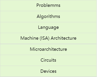
- Level of transformation
- Ambiguity that problems described by natural languages have would be unacceptable in instructions provided to a computer.
- So we should transform the natural language description of the problem to an algorithm first. An algorithm is a step-by-step procedure that is guaranteed to terminate, such taht each step is precisely stated and can be carried out by the computer.
- Here are terms to describe each of these properties:
- And we use the term definiteness to describe the notion that each step is precisely stated.
- We use the term effective computability to describe the notion that each step can be carried out by a computer.
- We use the term finiteness to describe the notion that the procedure terminates.
- Language
- high-level languages & low-level languages
- There is generally one low-level language tied to the computer on which the programs will execute, which is called assembly language for that computer.
- To tell the computer what to do in more underlying level, the program should be translated into the instruction set of the particular computer. The instruction set architecture (ISA) is the complete specification of the interface between programs that have been written and the underlying computer hardware that must carry out the work of those programs.
- Things below are specified by ISA:
- The term opcode is used to describe the operation.
- The term operand is used to describe individual data values.
- The ISA specifies the acceptable representations for operands which are called data types. It’s a representation of an operand such that the computer can perform operations on that representation.
- Mechanisms that the computer can use to figure out where the operands are located are called addressing modes.
- The ISA also specifies the number of unique locations that comprise the computer’s memory and the number of individual 0s and 1s that are contained in each location.
- The ISA specifies the memory organization, register set, and instruction set, including the opcodes, data types, and addressing modes of the instructions in the instruction set. (See more in Chapter 5)
x86(IBM)``ARM``THUMB(ARM)``PowerPC(IBM & Motorola)``z/Architecture(IBM)``SPARC(Oracle)- The translation from a high-level language to the ISA of the computer on which the program will execute is usually done by compiler, and the translation from the unique assembly language of a computer to its ISA is done by an assembler.
- Microarchitecture (or implementation) is the digital logic that allows an instruction set to be executed.
- A microarchitecture is the physical implementation of an instruction set.
- Each microarchitecture is an opportunity for computer designers to make different tradeoffs between the cost of the microprocessor, the performance that microprocessor will provide, and the microprocessor, the performance that the microprocessor will provide, and the energy that is required to power the microprocessor.
- eg: x86’s original implementation was 8086, followed by the 80286, 80386, 80486 in 1980s, Pentium IV microprocessor in 2001, and Skylake in 2015.
- The logic circuit
- The devices
Chapter 2 | Bits, Data Types, and Operations
- Bits ~ Binary Digit
0/1- With one wire, one can differentiate only two things.
- Data Types
- Unsigned Integers
- Signed Integers
- Logical Variable
- Float
- ASCII
- Each ISA has its own set of data types and its own set of instructions that can operate on those data types.
- In this book, we willl mainly use two data types:
- 🔗 2’s complement integers for representing positive and negative integers that we wish to perform arithmetic on;
- Specially for floating point data type (Greater Range & Lesss Precision):
- Most ISAs today specify more than one floating point data type. One of them, usually called float, consists of 32 bits, allocated as follows:
- 1 bit for the sign (positive or negative)
- 8 bits for the range (the exponent field)
- 23 bits for precision (the fraction field)
- As for 16 bits : 1 / 5 / 10- As for 64 bits : 1 / 11 / 52- They are mostly in normalized form:- - The reason why%22%20aria-hidden%3D%22true%22%3E%0A%20%3Cuse%20xlink%3Ahref%3D%22%23E1-MJMAIN-31%22%20x%3D%220%22%20y%3D%220%22%3E%3C%2Fuse%3E%0A%20%3Cuse%20xlink%3Ahref%3D%22%23E1-MJMAIN-2264%22%20x%3D%22778%22%20y%3D%220%22%3E%3C%2Fuse%3E%0A%20%3Cuse%20xlink%3Ahref%3D%22%23E1-MJMATHI-65%22%20x%3D%221834%22%20y%3D%220%22%3E%3C%2Fuse%3E%0A%20%3Cuse%20xlink%3Ahref%3D%22%23E1-MJMATHI-78%22%20x%3D%222301%22%20y%3D%220%22%3E%3C%2Fuse%3E%0A%20%3Cuse%20xlink%3Ahref%3D%22%23E1-MJMATHI-70%22%20x%3D%222873%22%20y%3D%220%22%3E%3C%2Fuse%3E%0A%20%3Cuse%20xlink%3Ahref%3D%22%23E1-MJMATHI-6F%22%20x%3D%223377%22%20y%3D%220%22%3E%3C%2Fuse%3E%0A%20%3Cuse%20xlink%3Ahref%3D%22%23E1-MJMATHI-6E%22%20x%3D%223862%22%20y%3D%220%22%3E%3C%2Fuse%3E%0A%20%3Cuse%20xlink%3Ahref%3D%22%23E1-MJMATHI-65%22%20x%3D%224463%22%20y%3D%220%22%3E%3C%2Fuse%3E%0A%20%3Cuse%20xlink%3Ahref%3D%22%23E1-MJMATHI-6E%22%20x%3D%224929%22%20y%3D%220%22%3E%3C%2Fuse%3E%0A%20%3Cuse%20xlink%3Ahref%3D%22%23E1-MJMATHI-74%22%20x%3D%225530%22%20y%3D%220%22%3E%3C%2Fuse%3E%0A%20%3Cuse%20xlink%3Ahref%3D%22%23E1-MJMAIN-2264%22%20x%3D%226169%22%20y%3D%220%22%3E%3C%2Fuse%3E%0A%3Cg%20transform%3D%22translate(7225%2C0)%22%3E%0A%20%3Cuse%20xlink%3Ahref%3D%22%23E1-MJMAIN-32%22%3E%3C%2Fuse%3E%0A%20%3Cuse%20xlink%3Ahref%3D%22%23E1-MJMAIN-35%22%20x%3D%22500%22%20y%3D%220%22%3E%3C%2Fuse%3E%0A%20%3Cuse%20xlink%3Ahref%3D%22%23E1-MJMAIN-34%22%20x%3D%221001%22%20y%3D%220%22%3E%3C%2Fuse%3E%0A%3C%2Fg%3E%0A%3C%2Fg%3E%0A%3C%2Fsvg%3E#card=math&code=1%5Cleq%20exponent%20%5Cleq%20254&id=QTx5y)is that:- `1111``1111`: Specially, **infinity **is represented by the **exponent** field containing **all** **1s** and the **fraction **field containing **all 0s**. It's **positive **infinity while the **sign bit is **`**0**` & **negative **infinity while the **sign bit is **`**1**`.- `0000``0000`: Specially, we represent **subnormal **numbers (very tiny) with an exponent field of `0000``0000`, and:
![📔 [大一暑假] 计算机系统概论 | Introduction to Computing Systems - 图3](/uploads/projects/isshikixiu@codes/7c4ee3467371bcb95443266fffd3cc34.svg)
- - - Others: if the exponent is `1111``1111`, but the fraction is not all 0s, then it referred to NaN.- **Normalized form** demands exactly one non-zero binary digit (i.e., the value 1). So we get 24-bit quantity from the 23 fraction bits.- The 8 exponent bits are encoded in what we call an **excess code**, named fro the notion that one can get the _real_ exponent by treating the code as an unsigned integer and subtracting the **excess **(sometimes called **bias**).- In IEEE Floating Point, that excess is 127 for 32-bit floating point number.- eg: An exponent field containing`1000``0110`=`134`corresponds to the exponent `134`-`127`=`7`- **ASCII codes** for representing characters that we wish to input a computer bia the keyboard or output from the computer bia a monitor;
- Operations on Bits - Part I: Arthmetic
- Addition and Subtraction
- Sign-extension (SEXT)
- The value of a positive number does not change if we extend the sign bit 0 as many bit positions to the left as desired. Similarly, the value of a negative number does not change by extending the sign bit 1 as many bit positions to the left as desired.
- Overflow
- Operations on Bits - Part II: Logical Operations
- AND
- OR
- NOT
- XOR / Exclusive-OR
- DeMorgan’s Laws
- “It’s not the case that both A and B are false.” = “At leaset one or A and B is true.”
- The Bit Vector
- An m-bit pattern where each bit has a liogical value independent of the other bits is called a bit vector.
- The most common use of the bit vector is bit mask.
- Another common use of the bit vector involves managing a complex system made up of several units, each of which is individually and independently either busy or available. So we could keep track of m units with a m-bit vector.
- Hexadecimal Notation
Chapter 3 | Digital Logic Structures
- The Transistor
- Most computers today or rather most microprocessors are constructed out of MOS (metal-oxide semiconductor) transistors.
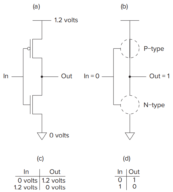
- It has two types: P-type & N-type. They both operate “logically”.
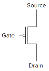
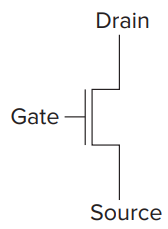
- Transistor has three terminals: the gate, the source and the drain.
- If the gate of the N-type transistor is supplied with:
- 1.2 volts: short circuit between the source and drain;
- 0 volts: open circuit between the source and drain;
- The P-type transistor works in exactly the opposite fashion from the N-type transistor, if the gate is supplied with:
- 0 volts: short circuit between the source and drain;
- 1.2 volts: open circuit between the source and drain;
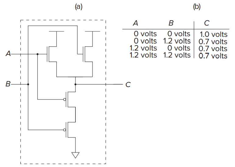
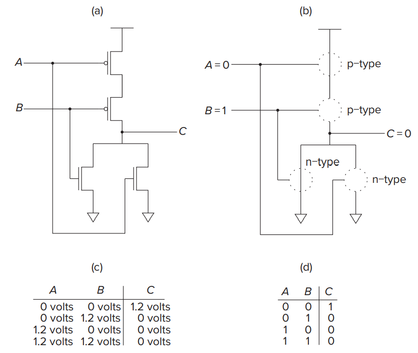
- We refer to circuits that contain both P-type and N-type transistors as CMOS (complementary metal-oxide semiconductor) circuits.
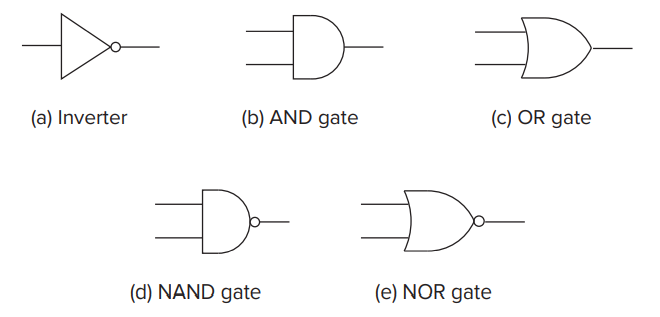
- Logic Gates
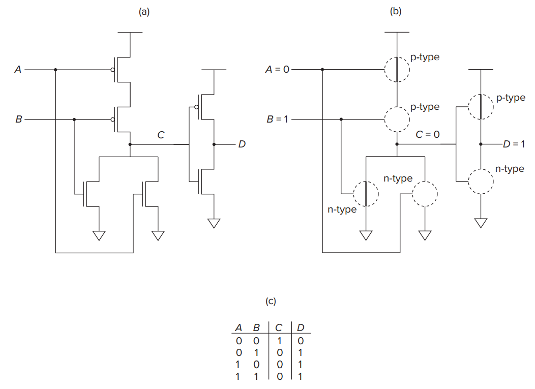
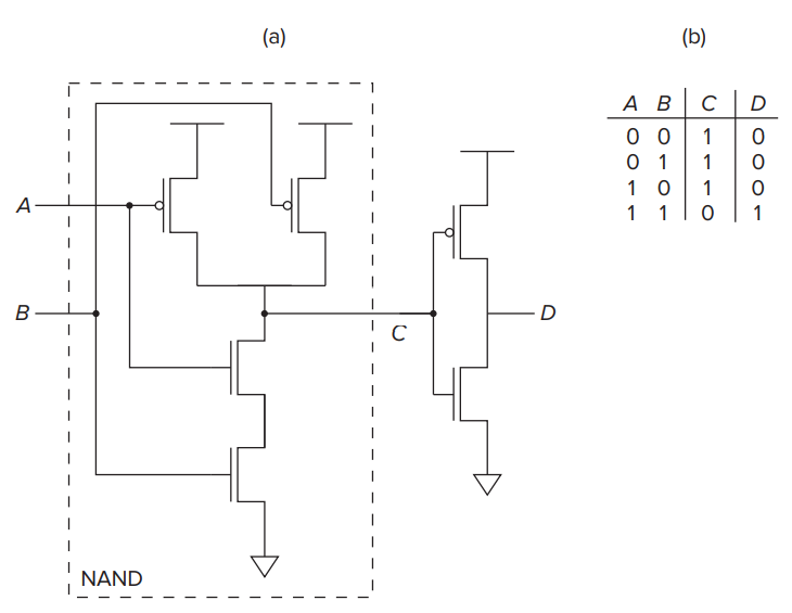
- Fundamentally two kinds of logic structures: those that include the storage of information and those that do not.
- Combinational Logic Circuits (do not store information).
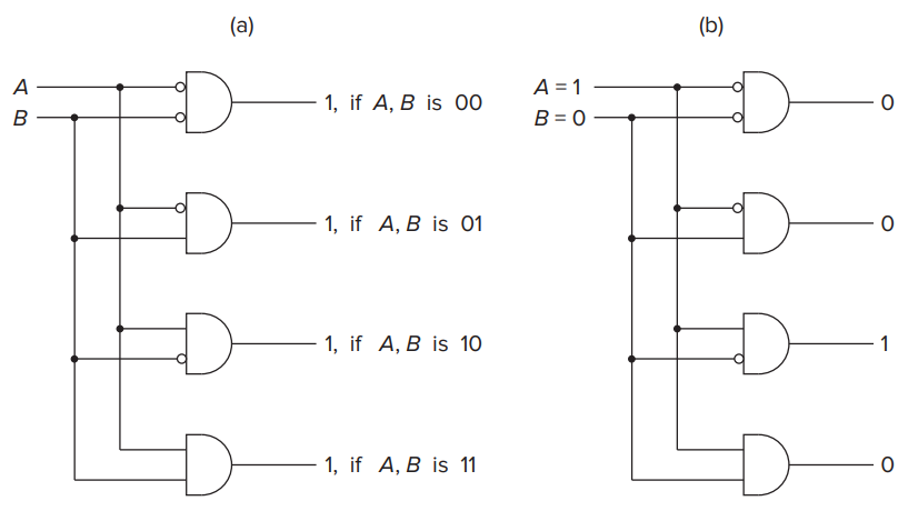
- Decoder
- Exactly one of its outputs is 1 and all the rest are 0s.
- In general, decoders have
inputs and
outputs.
- We say the output line that detects the input pattern is 🔗)asserted.
- The decoder is useful in determining how to interpret a bit pattern.
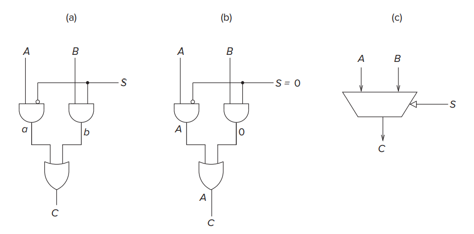
- Mux (multiplexer)
- The function of a mux is to select one of the inputs (A or B) and connect it to the output. The select signal (S in Figure 3.12) determines which input is connected to the output.
- We say S selects the source of the mux (either A or B) to be routed through to the output C.
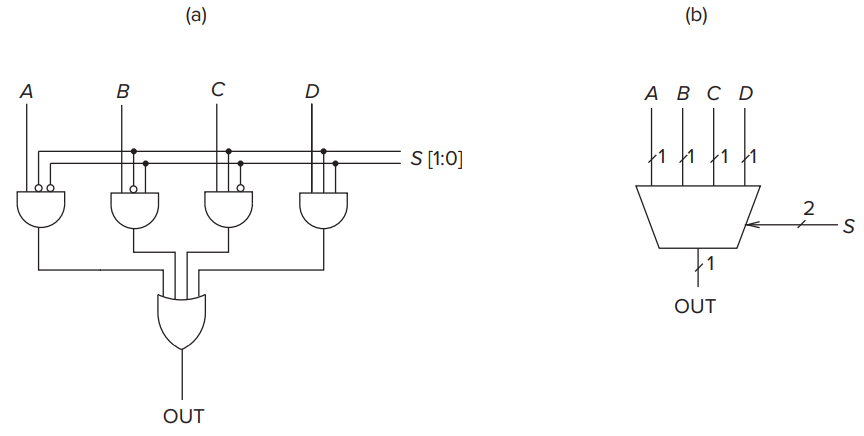
- In general, a mux consists of
inputs and
select lines.
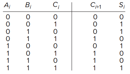
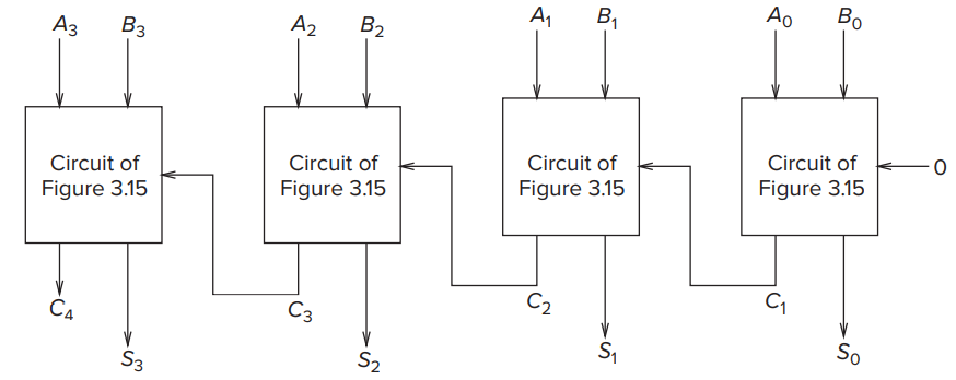
- One-bit Adder
- It describes the result of binary addition on one column of bits within two n-bit operands.
,
are digits from inputs,
is the carry number from
, and
is the
digit of output.
- Since the rightmost circuit depends on only two inputs (
), it has been referred to as a half adder.
- Since the other circuits depend on all three inputs (
), they are referred to as full adders.
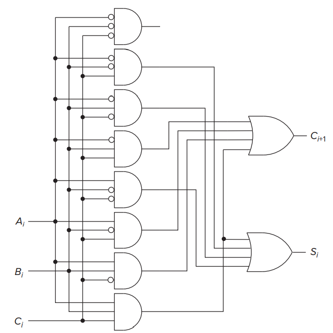
- The Programmable Logic Array (PLA)
- The implementation algorithm is simply to connect the output of an AND gate to the input of an OR gate if the corresponding row of the truth table produces an output 1 for that output column. Hence the notion of programmable. That is, we say we program the connections from AND gate outputs to OR gate inputs to implement our desired logic functions.
- Any logic function we wished to implement could be accomplished with a PLA.
- Logical Completeness
- We say that the set of gates {AND, OR, NOT} is logically complete because we can build a circuit to carry out the specification of any truth table we wish without using any other kind of gate.
- Basic Storage Elements
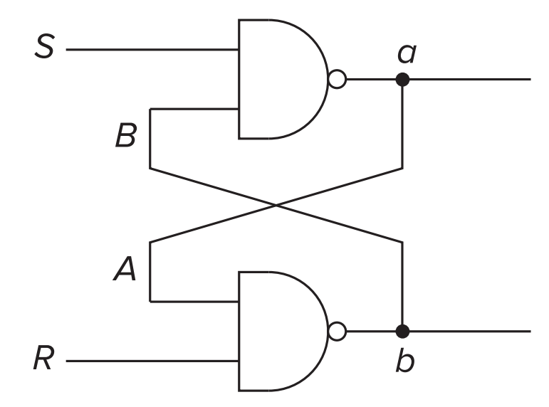
- R-S Latch
- R-S latch can store one bit of information.
- R : Resetting : setting the latch to store a
**0**;- S : Setting: setting the latch to store a
**1**;- The Quiescent (or quiet) State: the state when the latch is storing a value, either
0or1and nothing is try to change the value.
- When inputs S and R both have logic value
1.- At this time, the output of a and b won’t change. (But a and b are the opposite if we set S and R properly.)
- Setting the Latch to a
1or a0
- The latch can be set to a
1by momentarily setting S to0.- The latch can be set to a
0by momentarily setting R to0.- both S and R must never be allowed to be set to
0at the same time.- Tips: we ofen use the term clear to denote the act of setting a variable to 0.
- The Gated D Latch
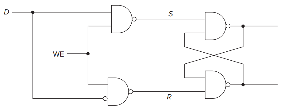
- To control when a latch is set and when it is cleared, a simple way is to use the gated latch.
- Setting the Latch to a
1or a0
- Only when WE (write enable) is asserted (i.e., when WE equals
1), latch can be set (to the value of D).- The Quiescent (or quiet) State
- When WE is not asserted (i.e., when WE equals
0), the outputs S and R are both equal to1.- The Comcept of Memory
- Memory is made up of a (usually large) number of locations, each uniquely identifiable and each having the ability to store a value.
- We refer to the unique identifier associated with each memory location as its address.
- Address Space
- kilo ~
- mega ~
- giga ~
- eg: 2 giga ->
exactly
- Addressability
- The number of bits stored in each memory location is the memory’s addressability.
- eg: A 2-gigabyte memory (2GB) is a memory consisting of
memory locations, each containing one byte (i.e., eight bits) of storage. Most memories are byte-addressable.
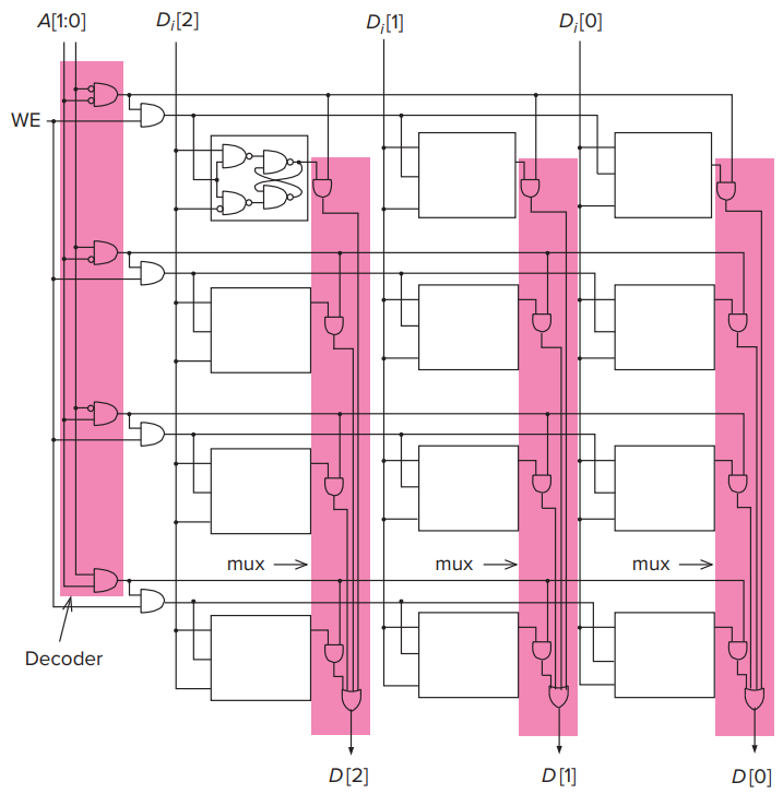
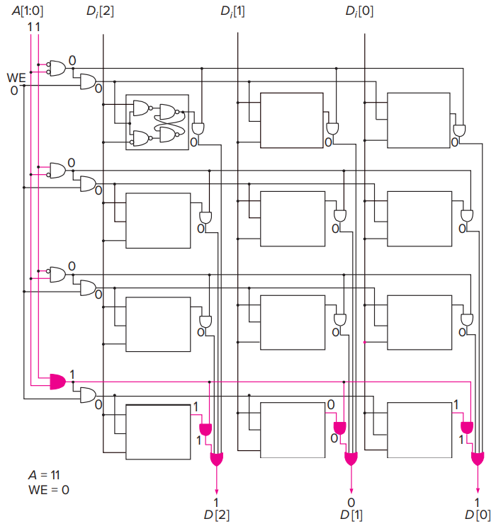
- A 22-by-3-Bit Memory
- That is, the memory has an address space of four locations and an addressability of three bits. It requires two bits to specify the address.
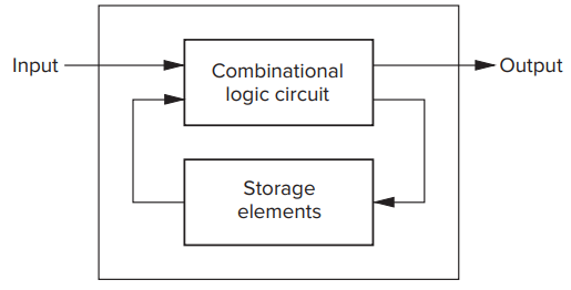
- Sequential Logic Circuits
- Can both process information and store information.
- Sequential logic circuits are used to implement a very important class of mechanisms called finite state machines, which are used in essentially all branches of engineering.
- eg: used as controllers of electrical systems, mechanical systems, and aeronautical systems.
- A Simple Example: The Lock
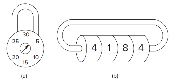
- Lock (a) will only open when you complete dialing in a specific order.- Assum that the correct order is R13-L22-R3.- Lock (b) won't care about how you complete rotation.
- The Concept of State
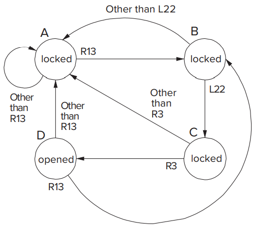
- Continue to take lock (a) for example, it identify the following situations (Each of these are the state of the lock.):
- Not open. No relevant operations have been performed;
- Not open. R13 completed.
- Not open. R13-L22 completed.
- Open. R13-L22-R3 completed.
- The notion of state is a very important concept. The state of a system is a snapshot of all relevant elements of the system at the moment that snapshot is taken.
- The Finite State Machine and Its State Diagram
- A finite state machine consists of five elements:
- a finite number of states
- a finite number of external inputs
- a finite number of external outputs
- an explicit specification of all state transitions
- an explicit specification of what determines each external output value
- Continue to take lock (a) for example:
- There is no fixed amount of time between successive inputs to the finite stat machine above. We say these systems are **asynchronous **because there is nothing synchronizing when each state transition must occur.
- The Synchronous Finite State Machine
- Computers are synchronous because the state transitions take place, one after the other, at identical fixed units of time, controlled by a synchronous finite state machine.
- Mealy machine & Moore machine
- The Clock
- Control of that synchronous behavior is in part the responsibility of the clock circuit.
- Each of the repeated sequence of identiacal intervals is referred to as a **clock cycle**.
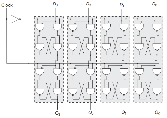
- The Flip-Flop
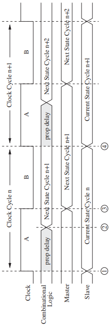
- The storage elements that allow us to read the current state throughout the current clock cycle, and not write the next state values into the storage elements until the beginning of the next clock cycle.
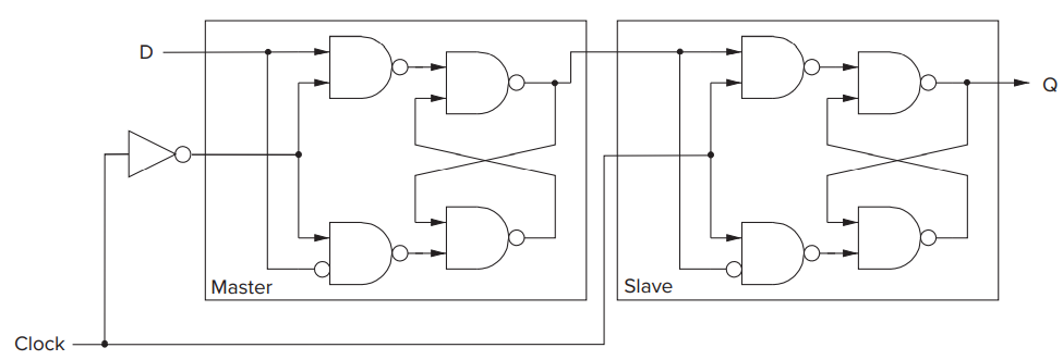
- Reading must be allowed throughout the clock cycle, and writing must occur at the end of the clock cycle.- The master / slave flip-flop can be constructed out of two gated D latches, one referred to as the master, the other referred to as the slave.- Think about that: When _master_ is "reading", the _slave_ is "writing", and vice versa.
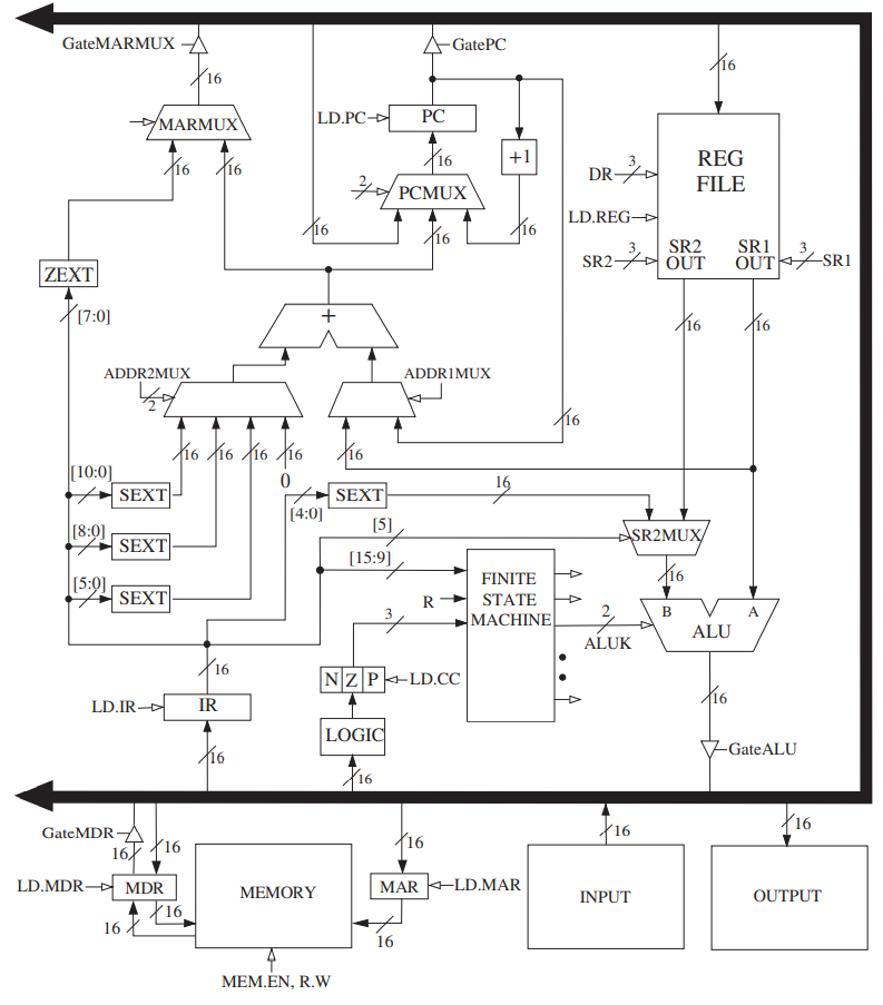
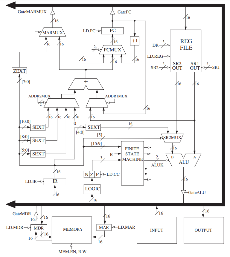
- Preview of Coming Attractions: The Data Path of the LC-3
- The data path consists of all the logic structures that combine to process information in the core of the computer.
- A register is simply a set of n _flip-flops that collectively are used to store one _n-bit value.
- In the figure, PC, IR, MAR, and MDR are all 16-bit registers that store 16 bits of information each. The block labeled REG FILE consists of eight registers that each store 16 bits of information.
- The data path also shows three 1-bit registers, N, Z, and P.
Chapter 4 | The von Neumann Model
- Basic Components
- To get a task done by a computer, we need:
- a computer program
- the computer
- The instruction is the smallest piece of work specified in a computer program.
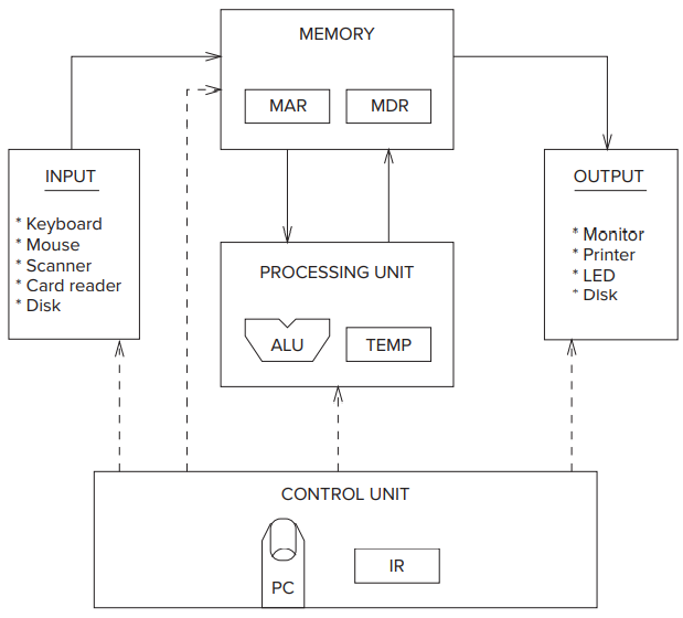
- John von Neumann proposed a fundamental model of a computer for processing computer programs in 1946. Here is it’s basic components:
- The von Neumann model consists of five parts: memory, a processing unit, input, output, and a control unit.
- The computer program is contained in the computer’s memory.
- The data the program needs to carry out the work of the program is either contained in the program’s memory or is obtained from the input devices.
- The results of the program’s execution are provided by the output devices.
- The order in which the instructions are carried out is performed by the control unit.
- Memory
- A typical memory in today’s world of computers consists of
distinct memory locations, each of which is capable of storing 8 bits of information.
- The memory address space of the LC-3 is
, and the addressability is 16 bits.
- To write (or store) a value in a memory location, we first write the address of the memory location in the MAR (memory’s address register), the value (interrogated from the computer’s memory) to be stored in the MDR (memory’s data register).
- The address of that location will be written to the (MAR) and then we interrogate the computer’s memory.
- The information stored in the location having that address will be placed in the memory’s data register (MDR).
- Processing Unit
- The processing unit carries out the actual processing of information in the computer.
- The processing unit in a modern computer can consist of many sophisticated complex functional units, each performing one particular operation (divide, square root, etc.).
- Simplest example: ALU (Arithmetic and Logic Unit).
- The ALU normally processes data elements of a fixed size referred to as the word length of the computer. The data elements are called words.
- Each ISA has its own word length, depending on the intended use of the computer.
- Most microprocessors today that are used in PCs or workstations have a word length of 64 bits (as is the case with Intel’s “Core” processors) or 32 bits (as is the case with Intel’s “Atom” processors). Even most microprocessors now used in cell phones have 64-bit word lengths, such as Apple’s A7 through A11 processors, and Qualcomm’s SnapDragon processors. However, the microprocessors used in very inexpensive applications often have word lengths of as little as 16 or even 8 bits.
- LC-3 has a word length of 16 bits.
- It is almost always the case that a computer provides some small amount of storage very close to the ALU to allow results to be temporarily stored if they will be needed to produce additional results in the near future. (They are important.)
- The most common form of temporary storage is a set of registers.
- Typically, the size of each register is identical to the size of values processed by the ALU; that is, they each contain one word.
- Current microprocessors typically contain 32 registers, each consisting of 32 or 64 bits, depending on the architecture.
- The LC-3 has eight registers (R0, R1, … R7), each containing 16 bits.
- Input & Output
- Control Unit
- It is the control unit that keeps track of both where we are within the process of executing the program and where we are in the process of executing each instruction.
- To keep track of which instruction is being executed, the control unit has an instruction register to contain that instruction.
- To keep track of which instruction is to be processed next, the control unit has a register that contains the next instruction’s address.
- For historical reasons, that register is called the PC (program counter), although a better name for it would be the instruction pointer.
- Curiously, Intel does in fact call that register the instruction pointer, but the simple elegance of that name has not caught on.
- The LC-3: An Example von Neumann Machine
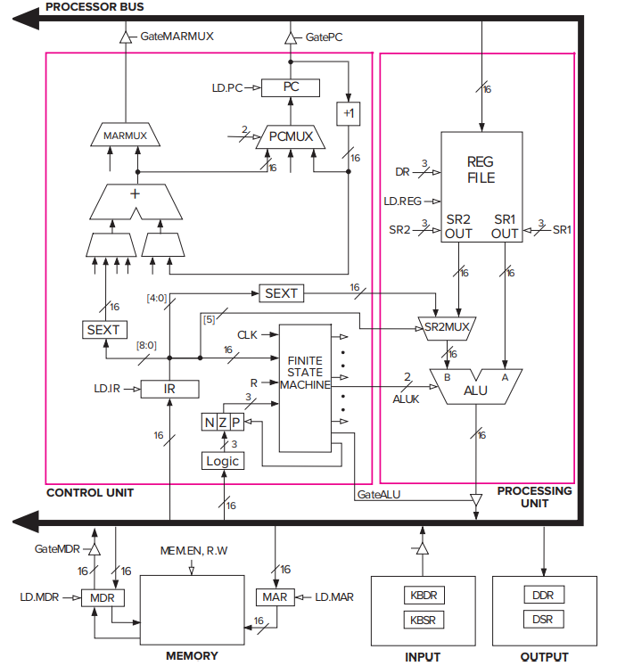
- Two kinds of arrowheads:
Filled-in: denote data elements that flow along the corresponding paths.
Not-filled in: denote control signals that control the processing of the data elements.
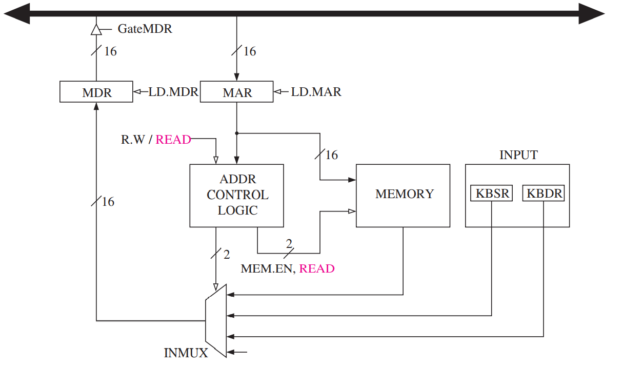
- MEMORY consists of the storage elements, along with the MAR for addressing individual locations and the MDR for holding the contents of a memory location on its way to/from the sotrage.
- NOTE: the MAR and MDR contains 16 bits, reflecting the fact that the memory address space of the LC-3 is
memory locations and the LC-3 is 16-bit addressable.
- INPUT/OUTPUT consists of a keyboard and a monitor.
- The simplest keyboard requires two registers: a KBDR (keyboard data register) for holding the ASCII codes of keys struck and a KBSR (keyboard status register) for maintaining status information about the keys struck.
- The simplest monitor requires two registers: a DDR (display data register) for holding the ASCII code of something to be displayed on the screen and a DSR (display status register) for maintaining associated status information.
- THE PROCESSING UNIT consists of a functional unit (ALU here) that performs arithmetic and logic operations and eight registers (R0, … R7) for storing temporary values that will be needed in the near future as operands for subsequent instructions.
- The LC-3 ALU can perform one arithmetic operation (addition) and two logical operations (bitwise AND and bitwise NOT).
- THE CONTROL UNIT consists of all the structures needed to manage the processing that is carried out by the computer.
- Its most important structure is the finite state machine, which directs all the activity.
- Note the CLK input to the finite state machine. It specifies how long each clock cycle lasts.
- The IR (instruction register) is also an input to the finite state machine since the LC-3 instruction being processed determines what activities must be carried out.
- The PC (program counter) is also a part of the control unit; it keeps track of the next instruction to be executed after the current instruction finishes.
- Note that all the external outputs of the finite state machine in the figure have arrowheads that are not filled in. These outputs control the processing throughout the computer.
- eg: ALUK: controls the operation performed in the ALU (ADD/AND/NOT) during the current clock cycle.
- eg: GateALU: determines whether or not the output of the ALU is provided to the processor bus during the current clock cycle.
- Instruction Processing
- The Instruction
- The most basic unit of computer processing, instruction, is made up of two parts: the opcode (what to do) and the operands (who it does to).
- Three fundamentally kinds of instructions: operates, data movement, and control. Although many ISAs have some special instructions that are necessary for those ISAs.
- Operate instructions operate one data.
- LC-3 has three operate instructions: ADD/AND/NOT
- Data movement instructions move information from the processing unit to and from memory and to and from input/output devices.
- The LC-3 has six data movement instructions.
- Control instructions are necessary for altering the sequential processing of instructions.
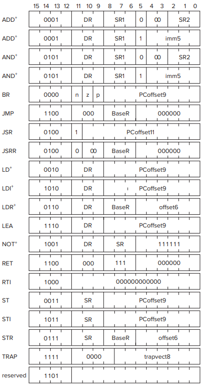
- An LC-3 instruction consists of 16 bits (one word), numbered from left to right, bit [15] to bit [0].
- Bits [15:12] contain the opcode. This means there are at most
distinct opcodes. Actually, we use only 15 of the possible four-bit codes. One is reserved for some future use.
- Bits [11:0] are used to figure out where the operands are.
**ADD**see docs**AND**see docs**LD**see docs- The Instruction Cycle (Not the Clock Cycle!)
- The instruction cycle is the entire sequence of steps needed to process an instruction.
- The instruction cycle consists of six esequential phases, each phase requiring zero (not all instructions require all six phases) or more steps.
- **FETCH**- The FETCH phase obtains the next instruction from memory and loads it into the **IR **(instruction register) of the control unit.- The **PC** contains the address of the next instruction to be processed.- So the FETCH do the following things:- Load the MAR with the contents of the PC, and simultaneously **increment** the **PC**. _[one clock cycle]_- Interrogate memory, resulting in the instruction being placed in the MDR. _[one clock cycle or more]_- Load the IR with the contents of the MDR. _[one clock cycle]_- Each of these steps is under the direction of the **control unit**.- **DECODE**- The DECODE phase examines the instruction in order to figure out what the microarchitecture is being asked to do.- **EVALUTE ADDRESS**- This phase computes the address of the memory location that is needed to process the instruction.- For instructions that needn't deal with an address (such as ADD with bits [5] = 0), the EVALUATE ADDRESS phase is not needed.- **FETCH OPERANDS**- This phase obtains the source operands needed to process the instruction.- **EXECUTE**- This phase carries out the execution of the instruction.- **STORE RESULT**- The final phase of an instruction's execution. The result is written to its designated destination.
- Changing the Sequence of Execution
- Control instructions perform that function by loading the PC during the EXECUTE phase, which wipes out the incremented PC that was loaded during the FETCH phase.
**BR**see docs- Control of the Instruction Cycle
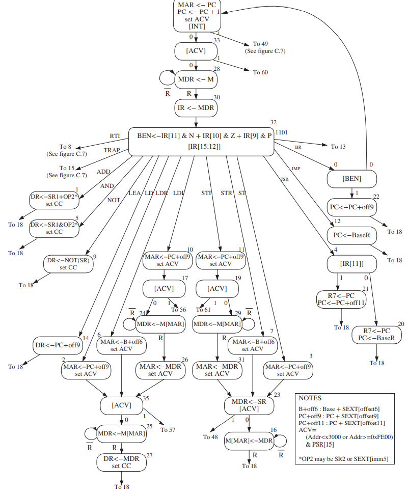
- The instrucion cycle is controlled by a synchronous finite state machine.
- Halting the Computer (the TRAP Instruction)
- If we need to stop this potentially infinite sequence of instruction cycles, we should stop the **clock**.- In the LC-3, as in many other machines, it is done under control of the operating system. For now it is enough to know that if a user program requires help from the operating system, it requests that help with the **TRAP **instruction (opcode = 1111) and an eight-bit code called a **trap vector**, which identifies the help that the user program needs. The eight-bit code** x25** tells the operating system that the program has finished executing and the computer can stop processing instructions.
- Our First Program: A Multiplication Algorithm
Chapter 5 | The LC-3
- The ISA: Overview
- The ISA specifies everything in the computer that is available to a programmer when he/she writes programs in the computer’s own machine language.
- The ISA specifies the memory organization, register set, and instruction set, including the opcodes, data types, and addressing modes of the instructions in the instruction set.
- Memory Organization
- Details in Chapter 9.
- Address space:
locations.
- Addressability:
bits.
- Word:
bits.
- word-addressable
- Registers
- Like almost all computers, LC-3 provides additional temporary storage locations that can be accessed in a single clock cycle, while it usually takes far more than one clock cycle to obtain data from memory.
- The most common type of temporary storage locations is a set of registers. Each in the set is called a GPR (general purpose register). Usually, the number of bits stored in each register is one word (
bits in LC-3).
- Registers must be uniquely identifiable. The LC-3 specifies eight GPRs, each identified by a three-bit register number. They are referred to as R0, R1, … R7.
- register file
- The Instruction Set
- Instruction is made up of two parts: the opcode (what to do) and the operands (who it does to).
- The instruction set is defined by its set of opcodes, data types, and addressing modes.
- The addressing modes determine where the operands are located.
- The data type is the representation of the operands in 0s and 1s.
- Opcodes
- Some ISAs have a very large number of opcodes, one for each of a very large number of tasks that a program may wish to carry out.
- There are three different types of instructions, which means three different types of opcodes: operates, data movement, and control.
- Operate instructions process information.
- Data movement instructions move information between memory and the registers and between registers/memory and input/output devices.
- Control instructions change the sequence of instructions that will be executed.
- Data Types
- Every opcode will interpret the bit patterns of its operands according to the data type it is designed to support.
- Addressing Modes
- An addressing mode is a mechanism for specifying where the operand is located.
- LC-3 supports five addressing modes:
- immediate/literal (the same)
- register
- 3 memory addressing modes:
- PC-relative
- indirect
- Base+offset
- Condition Codes
- The LC-3 has three single-bit registers that are individually set (set to 1) or cleared (set to 0) each time one of the eight general purpose registers is written into as a result of execution of one of the operate instructions or one of the load instructions.
- Each operate instruction performs a computation and writes the result into a general purpose register.
- Each load instruction reads the contents of a memory location and writes the value found there into a general purpose register.
- The three single-bit registers are called N, Z, and P, corresponding to their meaning: negative, zero, and positive. And their value will be modified each time a GPR is written by an operate or a load instruction.
- They are referred to as condition codes because the condition of those bits are used to change the sequence of execution of the instructions in a computer program. (e.g.
BR‘s condition.)
- Operate Instructions
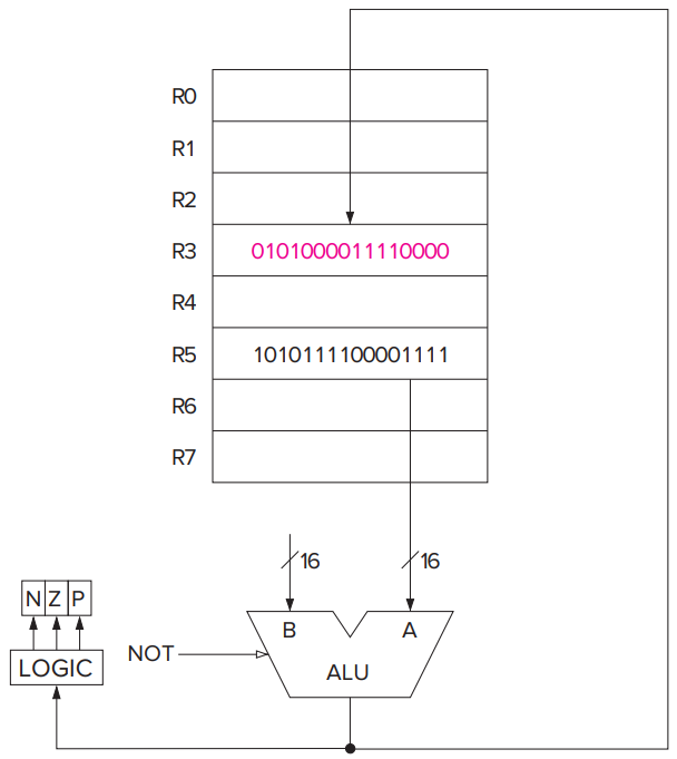
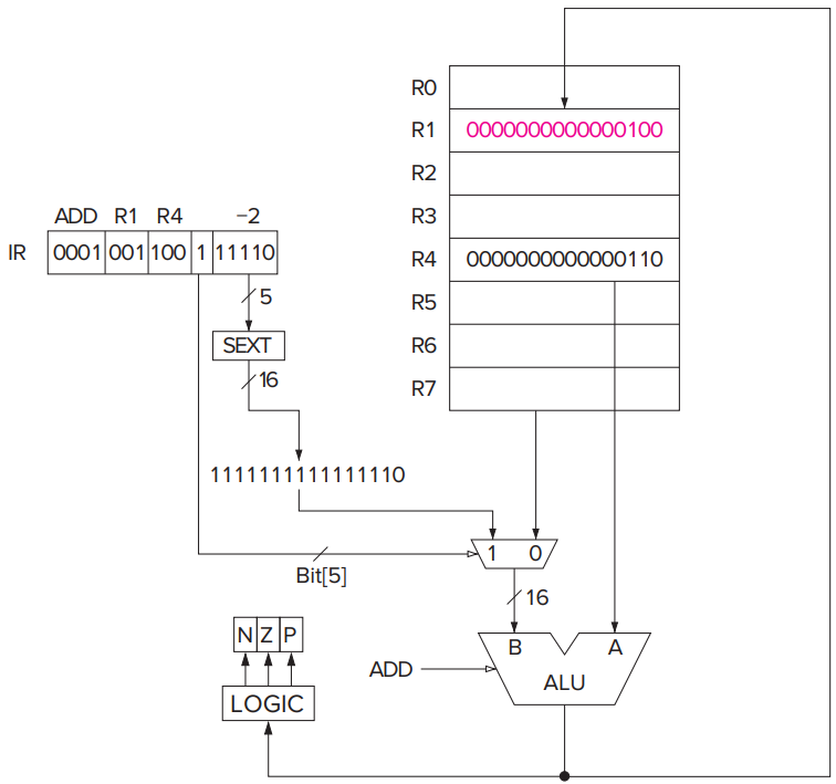
**ADD**,**AND**, and**NOT**- The
**NOT**(opcode = 1001) instruction is the only (in LC-3) operate instruction that performs a unary operation. See docs for details.
- Immediates
- Since the immediate operand havs a size less than a word, so not all 2's complement integers can be immediate operands.
- The LEA Instruction (Although Not Really an Operate)
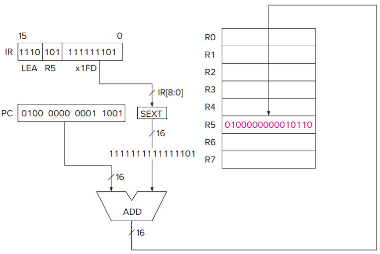
- It does not really operate on data, it simply loads a register with an address. It clearly does not move data from memory to a register, nor is it a control instruction. We had to put it somewhere, so we chose to discuss it here! See docs for details.
- We shall see shortly that the LEA instruction is useful to **initialize **a register with an address that is very close to the address of the instruction doing the initializing.
- Data Movement Instructions
- We will ignore for now the business of moving information from input devices to registers and from registers to output devices which will be an important part of Chapter 9. In this chapter, we will confine ourselves to moving information between memory and the general purpose registers.
- The process of moving information from memory to a register is called a load.
- The process of moving information from a register to memory is called a store.
- In both cases, the information in the location containing the source operand remains unchanged.
- In both cases, the location of the destination operand is overwritten.
- The LC-3 contains six instructions that move information:
**LD**,**LDR**,**LDI**;**ST**,**STR**,**STI**.
- Data movement instructions require two operands, a source and a destination.
- PC-Relative Mode
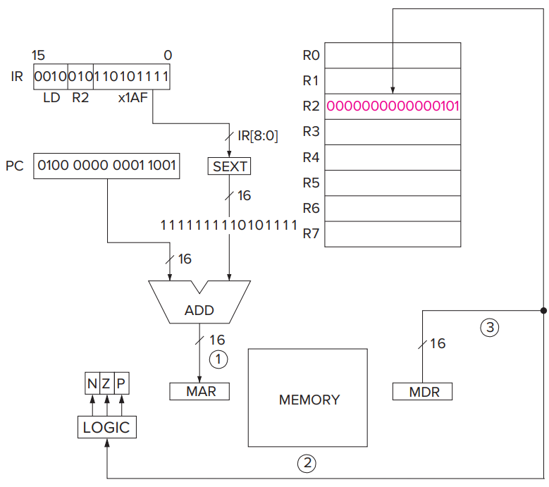
**LD**and**ST**specify the PC-relative addressing mode.
- Indirect Mode
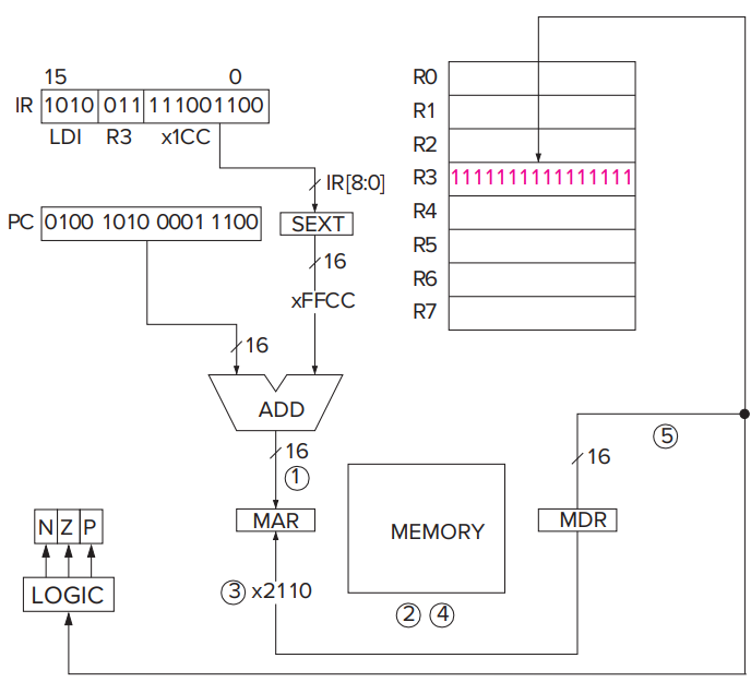
**LDI**and**STI**specify the indirect addressing mode that means the address of the address of the operand to be loaded or stored.
- Base+offset Mode
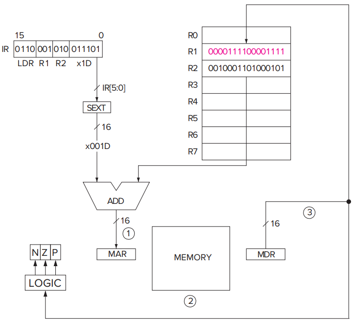
LDRandSTRspecify the Base+offset addressing mode. The Base+offset mode is so named because the address of the operand is obtained by adding a sign-extended six-bit offset to a base register.
- Note that the Base+offset addressing mode also allows the address of the operand to be **anywhere **in the computer's memory.
- An example.
- Control Instructions
- The LC-3 has five opcodes that enable the sequential execution flow to be broken:
- conditional branch
- unconditional jump
- subroutine call (sometimes called function
**TRAP**(service call)**RTI**(Return from Trap or Interrupt)- Conditional Branches
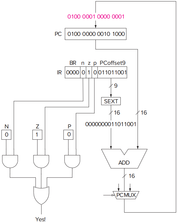
**BR**See docs for details.
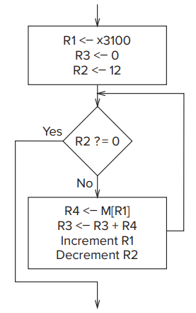
- Two Methods of Loop Control
- loop body & iteration fo the loop body
- Loop Control with a Counter
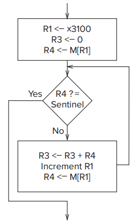
- Loop Control with a Sentinel
- We append to our sequence of values to be processed a value that we know ahead of time can never occur (i.e., the sentinel).
- eg: if we are adding a sequence of numbers, a sentinel could be a letter
Aor a*, that is, something that is not a number.
- The
**JMP**Instruction. See docs for details.- The
**TRAP**Instruction. See docs for details.
- The
**TRAP**instruction changes the PC to a memory address that is part of the operating system so that the operating system will perform some task on behalf of the program that is executing.- In the language of operating system jargon, we say the
**TRAP**instruction invokes an operating system service call. Bits [7:0] of the**TRAP**instruction form the trapvector, an eight-bit code that identifies the service call that the program wishes the operating system to perform on its behalf.
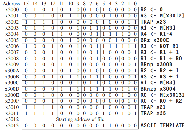
- Another Example: Counting Occurrences of a Character
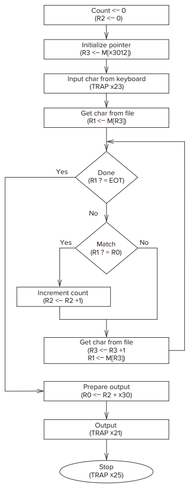
- The Data Path Revisited
- Basic Components of the Data Path
- The Global Bus
- The LC-3 global bus consists of 16 wires and associated electronics. It allows one structure to transfer up to 16 bits of information to another structure by making the necessary electronic connections on the bus.
- Note that each structure that supplies values to the bus has a triangle just behind its input arrow to the bus. This triangle (called a tri-state device) allows the computer’s control logic to enable exactly one supplier to provide information to the bus at any one time.
- The pros and cons of a single global bus is yet another topic that will have to wait for later in your education.
- Memory
- One of the most important parts of any computer is the memory that contains both instructions and data.
- Memory is accessed by loading the memory address register (MAR) with the address of the location to be accessed. To perform a load, control signals then read the contents of that memory location, and the result of that read is delivered by the memory to the memory data register (MDR). On the other hand, to perform a store, what is to be stored is loaded into the MDR. Then the control signals assert a write enable (WE) signal in order to store the value contained in MDR in the memory location specified by MAR.
- The ALU and the Register File
- The results of an ALU operation are (a) a result that is stored in one of the registers, and (b) the three single-bit condition codes.
- The PC and the PCMUX
- The MARMUX
- The Instruction Cycle Specific to the LC-3
- FETCH
- DECODE
- EVALUATE ADDRESS
- OPERAND FETCH
- EXECUTE
- STORE RESULT
Chapter 6 | Programing
- Problem Solving
- Systematic Decomposition
Chapter 7 | Assembly Language
- The mechanical language can be more user-friendly.
- We generally partition mechanical languages into two classes, high-level and low-level.
- Before a program written in a high-level language can be executed, it must be translated into a program in the ISA of the computer on which it is expected to execute.
- Assembly language is a low-level language.
- Low-level languages are very much ISA dependent. In fact, it is usually the case that each ISA has only one assembly language.
- Assembly languages let us use mnemonic devices for opcodes, such as ADD for
0001and NOT for1001, and they let us give meaningful symbolic names to memory locations that are called symbolic addresses, such as SUM or PRODUCT, rather than use the memory locations’ 16-bit addresses.- An Assembly Language Program
- The translation program is called an assembler, and the translation process is called assembly.
- In LC-3 ISA, an instruction in assembly language consists of four parts:
Label Opcode Operands ; Comment- *Label & Comment are optional, Opcode & Operands are mandatory.
- Opcode & Operands
- The Opcode is a symbolic name for the opcode of the corresponding LC-3 instruction.
- The number of operands depends on the operation being performed.
- A literal value must contain a symbol identifying the representation base of the number. We use
#for decimal,xfor hexadecimal, andbfor binary.- Labels
- Labels are symbolic names that are used to identify memory locations that are referred to explicitly in the program.
- In LC-3 assembly language, a label consists of from 1 to 20 alphanumeric characters (i.e., each character is a capital or lower-case letter of the English alphabet, or a decimal digit), starting with a letter of the alphabet except reserved words.
- There are two reasons for explicitly referring to a memory location:
- The location is the target of a branch instruction.
- The location contains a value that is loaded or stored.
- Comments
- The purpose of comments is to make the program more comprehensible to the human reader.
- Pseudo-Ops (Assembler Directives)
- Pseudo-ops help the assembler perform the task that translates the program in machine language into a program in the ISA.
- The LC-3 assembly language contains five pseudo-ops that we will find useful in our assembly language programming:
**.ORIG**,**.FILL**,**.BLKW**,**.STRINGZ**, and**.END**. All are easily recognizable by the dot as their first character.**.ORIG**
- It tells the assembler where in memory to place the LC-3 program.
**.FILL**
- It tells the assembler to set aside the next location in the program and initialize it with the value of the operand. The value can be either a number or a label.
**.BLKW**
- It tells the assembler to set aside some number of sequential memory locations (i.e., a BLocK of Words) in the program. The actual number is the operand of the .BLKW pseudo-op.
**.STRINGZ**
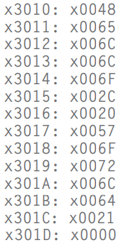
- It tells the assembler to initialize a sequence of n+1 memory locations. The argument is a sequence of n characters inside double quotation marks.
- eg:
It would result in the assembler initializing locations
x3010throughx301Dto the following values:
- `**.END**`- `**.END**` tells the assembler it has reached the end of the program and need **not even look at anything after it**. That is, any characters that come after `.END` will **not be processed** by the assembler.- `**.END**` does **not** **stop **the program during execution. In fact, `**.END**` does **not **even **exist **at the time of execution.
- Example: The Character Count Example of Section 5.5, Revisited Again.
- The Assembly Process
- Introduction
- If you have available an LC-3 assembler, you can cause it to translate your assembly language program into a machine language program by executing an appropriate command. In the LC-3 assembler that is generally available via the web, that command is assemble, and it requires as an argument the filename of your assembly language program.
- eg:
assemble solution1.asm outfile- A Two-Pass Process
- The objective of the first pass is to identify the actual binary addresses corresponding to the symbolic names (or labels). This set of correspondences is known as the symbol table.
- In pass 1, we construct the symbol table. In pass 2, we translate the individual assembly language instructions into their corresponding machine language instructions.
- The First Pass: Creating the Symbol Table
- The Second Pass: Generating the Machine Language Program
Chapter 8 | Data Structures
- Stack
- Linked List
- Queue
- Characters String
Chapter 9 | I/O
- The more generic term for our TRAP instruction is system call because the TRAP instruction is calling on the operating system to do something for us while allowing us to remain completely clueless as to how it gets done.
- Operating systems have the same goal: to optimize the use of all the resources of the computer system while making sure that no software does harmful things to any program or data that it has no right to mess with.
- Privilege, Priority, and the Memory Address Space
- Privilege and Priority
- Privilege
- Privilege is all about the right to do something, such as execute a particular instruction or access a particular memory location.
- Not all computer programs have the right to execute all instructions.
- We designate every computer program as either privileged or unprivileged.
- We say a program is executing in Supervisor mode to indicate privileged, or User mode to indicate unprivileged.
- If a program is executing in Supervisor mode, it can execute all instructions and access all of memory.
- If a program is executing in User mode, it cannot.
- Priority
- Priority is all about the urgency of a program to execute.
- Every program is assigned a priority, specifying its urgency as compared to all other programs. This allows programs of greater urgency to interrupt programs of lesser urgency.
- Two Orthogonal Notions
- We said privilege and priority are two orthogonal notions, meaning they have nothing to do with each other.
- The Processor Status Register (PSR)
- Esch program executing on the computer has associated with it two very important registers, the Program Counter (PC) and the Processor Status Register (PSR) that is shown in figure below. It contains the privilege and priority assigned to that program.
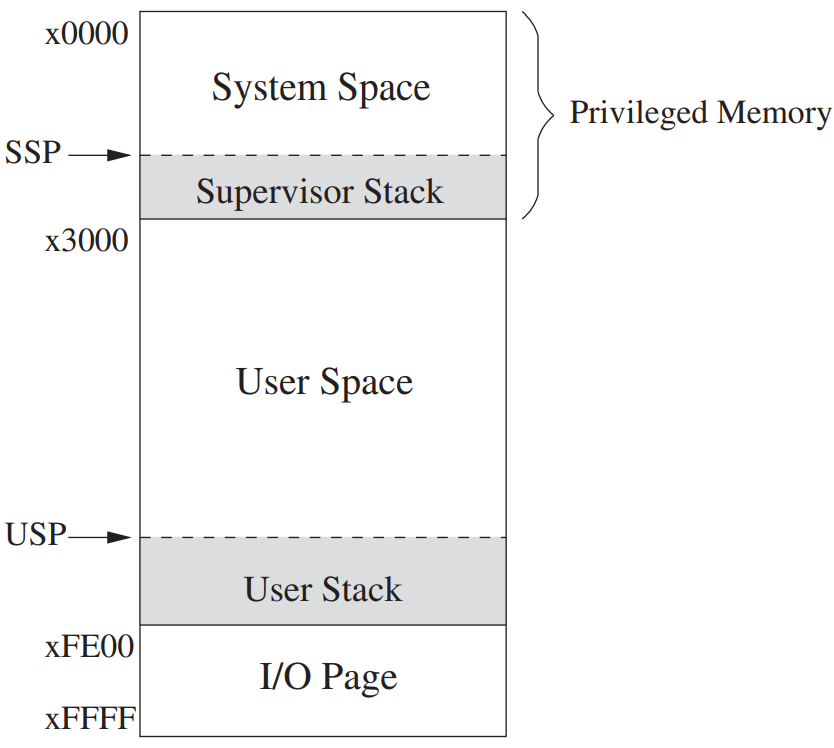
- Organization of Memory- **System Space** are **privileged **memory locations, which contain the various data structures and code of the operating system. Thery require **supervisor **privilege to access.- **Supervisor Stack** is controlled by the operating system and requires **supervisor **privilege to access. It has a stack pointer called **SSP** (Supervisor Stack Pointer).- **User Space** are **unprivileged **memory locations. Supervisor privilege is not required to access these memory locations. All user programs and data use this region of memory.- **User Stack** is controlled by the user program and does **not require privilege** to access. It has a stack pointer called **USP** (User Stack Pointer).- Since a program can only execute in **Supervisor **mode or **User **mode at any one time, only **one** of the two stacks is active at any one time.- **R6 **is generally used as the **SP **for the active stack. Two registers, **Saved_SSP **and **Saved_USP**, are provided to save the **SP **not in use. When privilege changes, for example, from **Supervisor **mode to **User **mode, the **SP **is stored in **Saved_SSP**, and the **SP **is loaded from **Saved_USP**.
- Input/Output
- Even the simplest I/O devices usually need at least two registers: one to hold the data being transferred between the device and the computer, and one to indicate status information about the device.
- An example of status information is whether the device is available or is it still busy processing the most recent I/O task.
- Some Basic Characteristics of I/O
- Memory-Mapped I/O vs. **Special I/O Instructions**
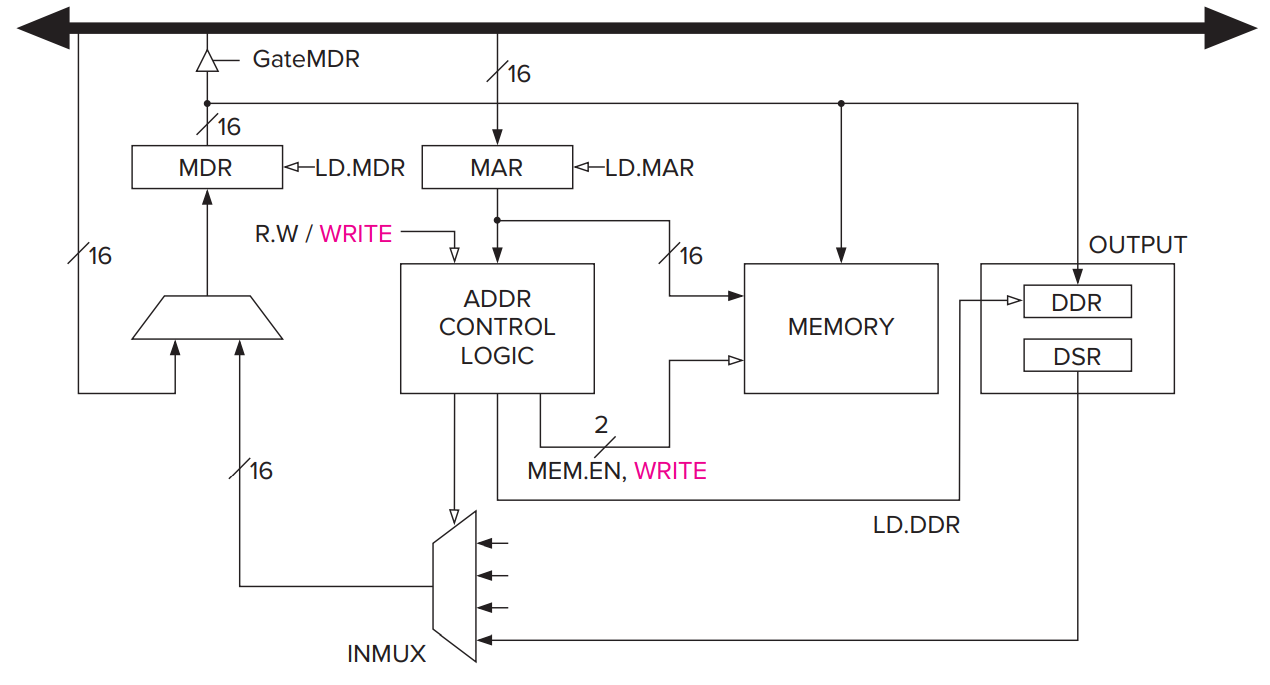
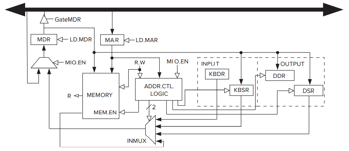
- The I/O device registers are mapped to a set of addresses that are allocated to I/O device registers rather than to memory locations. Hence the name memory-mapped I/O.
- Special I/O Instructions are not so liked.
- Asynchronous** vs. Synchronous**
- Most I/O is carried out at speeds very much slower than the speed of the processor.
- The point is that I/O devices usually operate at speeds very different from that of a microprocessor, and not in lockstep. We call this latter characteristic asynchronous. Most interaction between a processor and I/O is asynchronous.
- To control processing in an asynchronous world requires some protocol or handshaking mechanism. So it is with our keyboard and monitor.
- In the case of the keyboard, we will need a one-bit status register, called a flag, to indicate if someone has or has not typed a character.
- In the case of the monitor, we will need a one-bit status register to indicate whether or not the most recent character sent to the monitor has been displayed, and so the monitor can be given another character to display.
- These flags are the simplest form of synchronization.
- By examining the ready bit before reading a character, the computer can tell whether it has already read the last character typed.
- Interrupt-Driven vs. Polling
- 🔗 Difference between an interrupt and a trap.
- The processor, which is computing, and the typist, who is typing, are two separate entities.
- The issue of interrupt-driven vs. polling is the issue of who controls the interaction.
- Interrupt-driven acts like that the typist will tell the processor that there are some inputs.
- Polling acts like that the processor will interrogate typist again and again whether there have some inputs.
- Input from the Keyboard
- Basic Input Registers (KBDR and KBSR)
- KBDataR & KBStatusR
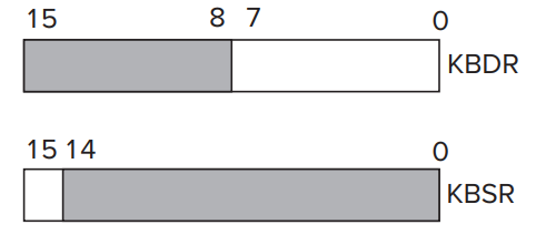
- In the case of KBDR, bits [7:0] are used for the data, and bits [15:8] contain
**x00**.- In the case of KBSR, bit [15] contains the synchronization mechanism, that is, the ready bit.
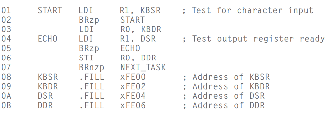
- In LC-3, address `**xFE02**`** **is assigned to the **KBDR**; address `**xFE00**`** **is assigned to the **KBSR**.- The Basic **Input Service Routine**- When type in something, **KBDR **is updated and **KBSR **is set to `1`. And **KBDR **can't be changed until **KBSR **is reset and the data in **KBDR **is read. So that each character can be loaded at least one time.
- Implementation of Memory-Mapped Input
- Output to the Monitor
- Basic Output Registers (DDR and DSR)
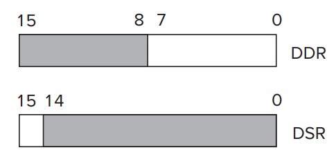
- In the case of DDR, bits [7:0] are used for data, and bits [15:8] contain
**x00**.- In the case of DSR, bit [15] contains the synchronization mechanism, that is, the ready bit.
- In LC-3, address `**xFE06**`** **is assigned to the **DDR**; address `**xFE04**` is assigned to the **DSR**.- The Basic Output Service Routine- When display something, **DDR **is updated and **DSR **is cleared. And **DDR **can't be changed until **DSR **is set to `1` and the data in **DDR **is printed.
- Implementation of Memory-Mapped Output
- Example: Keyboard Echo
- A More Sophisticated Input Routine
- Just print a prompt while reading.
- Implementation of Memory-Mapped I/O, Revisited
- Operating System Service Routines (LC-3 Trap Routines)
- In general it is ill-advised to give user programmers access to these registers. That is why the addresses of hardware registers are part of the privileged memory address space and accessible only to programs that have supervisor privilege.
- The simpler solution, as well as the safer solution to the problem of user programs requiring I/O, involves the
**TRAP**instruction and the operating system, which of course has supervisor privilege.- It (
**TRAP**) allows the user programmer to not have to know the gory details of I/O discussed earlier in this chapter. In addition, it protects user programs from the consequences of other inept user programmers.- The user program uses the
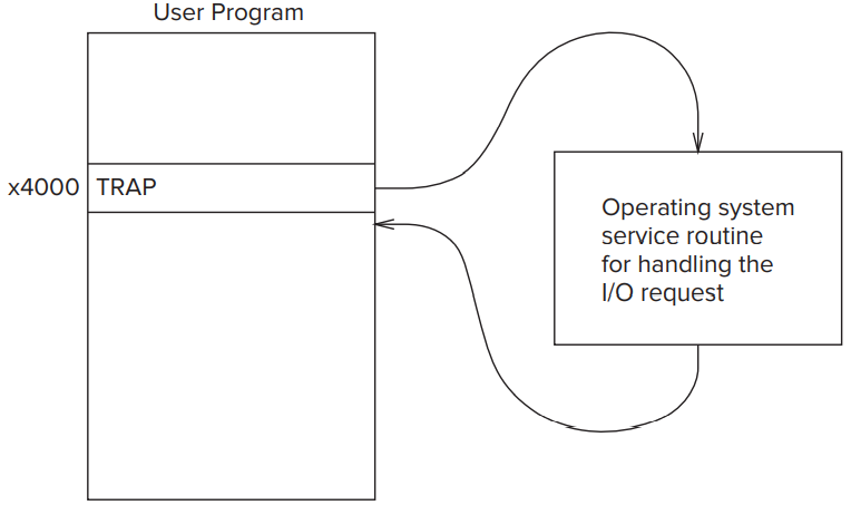
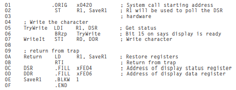
**TRAP**instruction to request the operating system to perform the task on behalf of the user program. The operating system takes control of the computer, handles the request specified by the**TRAP**instruction, and then returns control back to the user program at locationx4001. As we said at the start of this chapter, we usually refer to the request made by the user program as a system call or a service call.
- The Trap Mechanism
- A set of service routines executed on behalf of user programs by the operating system. These are part of the operating system and start at arbitrary addresses in system space. The LC-3 was designed so that up to 256 service routines can be specified. Table A.2 in Appendix A contains the LC-3’s current complete list of operating system service routines.
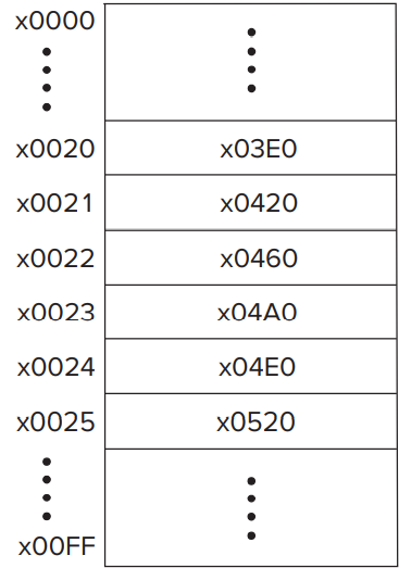
- A table of the starting addresses of these 256 service routines. This table is stored in memory locations x0000 to x00FF. The table is referred to by various names by various companies. One company calls this table the System Control Block. Another company calls it the Trap Vector Table. Figure 9.10 shows the Trap Vector Table of the LC-3, with specific starting addresses highlighted. Among the starting addresses are the one for the character output service routine (memory location x0420), which is stored in memory location x0021, the one for the keyboard input service routine (location x04A0), stored in location x0023, and the one for the machine halt service routine (location x0520), stored in location x0025.
- The
**TRAP**instruction. When a user program wishes to have the operating system execute a specific service routine on behalf of the user program, and then return control to the user program, the user program uses the TRAP instruction.- A linkage back to the user program. The service routine must have a mechanism for returning control to the user program.
- The TRAP Instruction
- The TRAP instruction causes the service routine to execute by:
- changing the
**PC**to the starting address of the relevant service routine on the basis of its trap vector;- providing a way to get back to the program that executed the
**TRAP**instruction. The “way back” is referred to as a linkage;- As you know, the
**TRAP**instruction is made up of two parts: the**TRAP**opcode 1111 and the trap vector (bits [7:0]), which identifies the service routine the user program wants the operating system to execute on its behalf. Bits [11:8] must be zero.
- The EXECUTE phase of the TRAP instruction’s instruction cycle does three things:
- The PSR and PC are both pushed onto the system stack. Since the PC was incremented during the FETCH phase of the TRAP instruction’s instruction cycle, the return linkage is automatically saved in the PC. When control returns to the user program, the PC will automatically be pointing to the instruction following the TRAP instruction. Note that the program requesting the trap service routine can be running either in Supervisor mode or in User mode. If in User mode, R6, the stack pointer, is pointing to the user stack. Before the PSR and PC can be pushed onto the system stack, the current contents of R6 must be stored in Saved USP, and the contents of Saved SSP loaded into R6.
- PSR[15] is set to 0, since the service routine is going to require supervisor privilege to execute. PSR[10:8] are left unchanged since the priority of the TRAP routine is the same as the priority of the program that requested it.
- The 8-bit trap vector is zero-extended to 16 bits to form an address that corresponds to a location in the Trap Vector Table. For the trap vector x23, that address is x0023. Memory location x0023 contains x04A0, the starting address of the TRAP x23 service routine. The PC is loaded with x04A0, completing the instruction cycle.
- The
**RTI**Instruction: To Return Control to the Calling Program
- The
**RTI**instruction (opcode = 1000, with no operands) pops the top two values on the system stack into the PC and PSR. Since the PC contains the address following the address of the TRAP instruction, control returns to the user program at the correct address.- Finally, once the PSR has been popped off the system stack,
**PSR[15]**must be examined to see whether the processor was running in User mode or Supervisor mode when the TRAP instruction was executed.- A Summary of the Trap Service Routine Process
- Trap Routines for Handling I/O
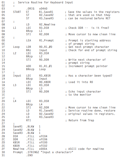
- A Trap Routine for Halting the Computer
- Interrupts and Interrupt-Driven I/O
- Interrupt-Driven I/O
- Two Parts to the Process
- Part I: Causing the Interrupt to Occur
- The Interrupt Signal from the Device
- The Urgency of the Request
- The INT Signal
- The Test for INT
- Part II: Handling the Interrupt Request
- Initiate the Interrupt
- Service the Interrupt
- Return from the Interrupt
- Not Just I/O Devices
- Polling Revisited, Now That We Know About Interrupts
- The Problem
- The Solution
