作业说明
Memory
要点提示
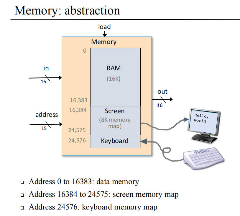
- 存储器分为三部分,分别为16K的RAM,8K的Screen和1Keyboard,根据他们的地址分配,可以观察通过高2位就能进行区分。(不过这里我好久不写HDL了,有些忘了这个地址结构)
- 访问16K的RAM,只需要低14位;访问8K的Screen只需要低13位。我一开始下意识就觉得地址是16位,调试了好久,才发现错误。
- 整体框架,之前写过类似的,先用
Dmux分配load,最后使用Mux选择输出。
// This file is part of www.nand2tetris.org// and the book "The Elements of Computing Systems"// by Nisan and Schocken, MIT Press.// File name: projects/05/Memory.hdl/*** The complete address space of the Hack computer's memory,* including RAM and memory-mapped I/O.* The chip facilitates read and write operations, as follows:* Read: out(t) = Memory[address(t)](t)* Write: if load(t-1) then Memory[address(t-1)](t) = in(t-1)* In words: the chip always outputs the value stored at the memory* location specified by address. If load==1, the in value is loaded* into the memory location specified by address. This value becomes* available through the out output from the next time step onward.* Address space rules:* Only the upper 16K+8K+1 words of the Memory chip are used.* Access to address>0x6000 is invalid. Access to any address in* the range 0x4000-0x5FFF results in accessing the screen memory* map. Access to address 0x6000 results in accessing the keyboard* memory map. The behavior in these addresses is described in the* Screen and Keyboard chip specifications given in the book.*//*00 ~ 3F --> 000 0000 ~ 011 111140 ~ 5F --> 100 0000 ~ 101 111160 --> 110 0000*/CHIP Memory {IN in[16], load, address[15];OUT out[16];PARTS:// Put your code here:DMux4Way(in=load, sel=address[13..14], a=loada, b=loadb, c=loadscr, d=loadkbd);Or(a=loada, b=loadb, out=loadram); //00 or 01 is access RAMRAM16K(in=in, load=loadram,address=address[0..13], out=outram);Screen(in=in, load=loadscr, address=address[0..12], out=outscr);Keyboard(out=outkbd);Mux4Way16(a=outram, b=outram, c=outscr, d=outkbd, sel=address[13..14], out=out);}
keyboard test
中间有两次键盘测试,需要切换View,为Screen,然后使用键盘按键,第一次为K,第二次为Y,区分大小写。
论坛中,有个人给出了操作步骤。
To anyone facing the same problem… on the Hardware Simulator user interface, right above where you see the script executing the tests, there are three drop down boxes. The one furthest to the right which is labeled “View” is probably currently set to “Script.” Click the drop down and select “Screen,” and you will see an interface that has a keyboard icon. Click it and then hit the corresponding key to complete the test.
CPU
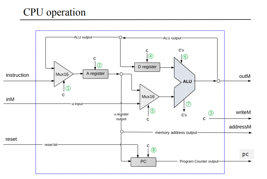
CPU: This chip can be constructed according to the proposed CPU implementation given in Figure 5.9 of Chapter 5, using the ALU and register chips built in Projects 2 and 3, respectively. We recommend though using built-in chip-parts instead, in particular ARegister and DRegister. The built-in versions of these two chips have exactly the same interface and functionality as those of the Register chip specified in Chapter 3; however, they feature GUI side-effects that come handy for testing purposes.
CPU设计的难点就在于控制信息的处理,好多处控制信息课程中没有明确给出。我也是在设计jump位时没有思路,参考别人的代码。当然,我前两部分的设计和“参考”思路不同,采用的类似前几周的分配思路。
控制位设计要点
下面我来分析一下CPU设计要点
- 第一个Mux如何选择输入?显然,对于A指令,希望把instruction读入A寄存器作为地址,当指令为C指令时,选择的则是ALU的
aluoutput; - A指令必定访问A寄存器,C指令根据指令的第5位判断是否访问A寄存器;
- A寄存器的输出是否写回存储器
writeM?A指令从不写回,C指令根据第3位判断; - D寄存器
D register、M寄存器inM和PC的跳转load的访问与A指令无关,因此当为A指令时,④⑤⑧控制位为false;④处控制信息,C指令根据第4位判断; - ⑤处控制信息,C指令根据第12位判断;
- ⑥处控制信息,C指令根据第6…11位进行判断;
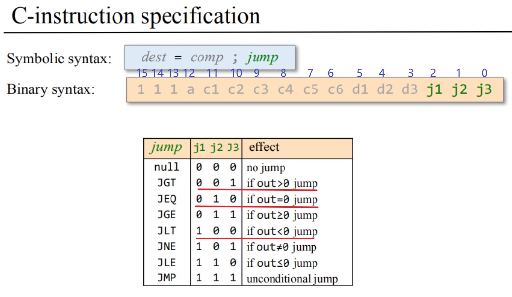
- ⑦处为ALU的符号输出位
ng和zr,分表表示负位和零位,并可以间接计算出正位。 - 将负位、零位和正位分别于C指令的
jmp位相与,均不为零(存在跳转)时,⑧处得出跳转控制位为true;
指令的每一位含义需要参考第四周的讲义,在课程网站可以下载。下图就是根据jmp位的含义,判断哪一位为正位、负位和零位;其他控制位也是类似。
Nand2Tetris week-4
我的代码
// This file is part of www.nand2tetris.org
// and the book "The Elements of Computing Systems"
// by Nisan and Schocken, MIT Press.
// File name: projects/05/CPU.hdl

/**
 * The Hack CPU (Central Processing unit), consisting of an ALU,
 * two registers named A and D, and a program counter named PC.
 * The CPU is designed to fetch and execute instructions written in
 * the Hack machine language. In particular, functions as follows:
 * Executes the inputted instruction according to the Hack machine
 * language specification. The D and A in the language specification
 * refer to CPU-resident registers, while M refers to the external
 * memory location addressed by A, i.e. to Memory[A]. The inM input
 * holds the value of this location. If the current instruction needs
 * to write a value to M, the value is placed in outM, the address
 * of the target location is placed in the addressM output, and the
 * writeM control bit is asserted. (When writeM==0, any value may
 * appear in outM). The outM and writeM outputs are combinational:
 * they are affected instantaneously by the execution of the current
 * instruction. The addressM and pc outputs are clocked: although they
 * are affected by the execution of the current instruction, they commit
 * to their new values only in the next time step. If reset==1 then the
 * CPU jumps to address 0 (i.e. pc is set to 0 in next time step) rather
 * than to the address resulting from executing the current instruction.
 */

CHIP CPU {

    IN  inM[16],         // M value input  (M = contents of RAM[A])
        instruction[16], // Instruction for execution
        reset;           // Signals whether to re-start the current
                         // program (reset==1) or continue executing
                         // the current program (reset==0).

    OUT outM[16],        // M value output
        writeM,          // Write to M?
        addressM[15],    // Address in data memory (of M)
        pc[15];          // address of next instruction

    PARTS:
    // Put your code here:
    /*
        if(instruction[15] == 0) A-instruction --> loadinst = 0
        else C-instruction loadinst = 1
    */
    And(a=true, b=instruction[15], out=loadinst); //A-instruction or C-instruction
    Mux16(a=instruction, b=aluoutput, sel=loadinst, out=outmux1); //A-inst instruction is an address
    /*
    C-inst: if(instruction[5] == 1) load A register;
    A-inst: always access A register
    */
    Mux(a=true, b=instruction[5], sel=loadinst, out=loadareg);
    ARegister(in=outmux1, load=loadareg, out[0..14]=addressM, out=outareg);

    Mux(a=false, b=instruction[4], sel=loadinst, out=loaddreg);
    DRegister(in=aluoutput, load=loaddreg, out=outdreg);

    Mux16(a=outareg, b=inM, sel=instruction[12], out=outmux2);
    ALU(x=outdreg, y=outmux2, zx=instruction[11], nx=instruction[10],
        zy=instruction[9], ny=instruction[8], f=instruction[7], no=instruction[6],
        out=aluoutput, out=outM, zr=aluzr, ng=alung);

    Mux(a=false, b=instruction[3], sel=loadinst, out=writeM);

    /*
        ng  zr  po
        1   0   0
        0   1   0
        0   0   1
        1   1   not exit
    */
    Or(a=alung, b=aluzr, out=ngorzr);
    Not(in=ngorzr, out=alupo);
    And(a=alung, b=instruction[2], out=cmp2);
    And(a=aluzr, b=instruction[1], out=cmp1);
    And(a=alupo, b=instruction[0], out=cmp0);
    Or(a=cmp0, b=cmp1, out=cmp01);
    Or(a=cmp01, b=cmp2, out=cmp012);
    /*
    C-inst: ALU sign bits & the c-inst jjj bits not equals 0
    A-inst: never jump
    */
    And(a=loadinst, b=cmp012, out=jmp);

    PC(in=outareg, load=jmp, inc=true, reset=reset, out[0..14]=pc);

}
Computer
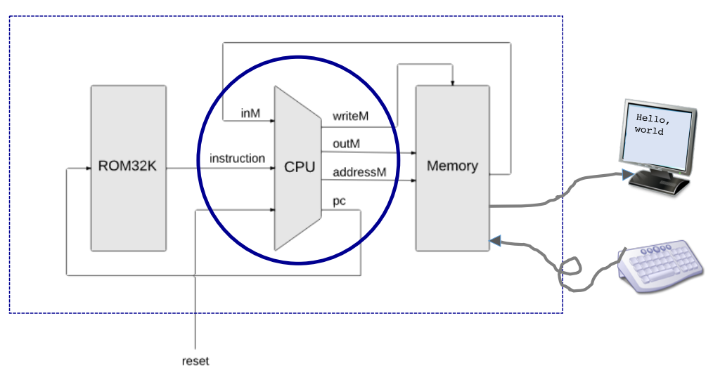
虽然没有说明接口怎么连,但根据数据线的宽度也能大致才出来一二。
// This file is part of www.nand2tetris.org
// and the book "The Elements of Computing Systems"
// by Nisan and Schocken, MIT Press.
// File name: projects/05/Computer.hdl

/**
 * The HACK computer, including CPU, ROM and RAM.
 * When reset is 0, the program stored in the computer's ROM executes.
 * When reset is 1, the execution of the program restarts.
 * Thus, to start a program's execution, reset must be pushed "up" (1)
 * and "down" (0). From this point onward the user is at the mercy of
 * the software. In particular, depending on the program's code, the
 * screen may show some output and the user may be able to interact
 * with the computer via the keyboard.
 */

CHIP Computer {

    IN reset;

    PARTS:
    // Put your code here:
    CPU(inM=inM, instruction=instruction, reset=reset,
        outM=outM, writeM=writeM, addressM=addressM, pc=pc);
    ROM32K(address=pc, out=instruction);
    Memory(in=outM, load=writeM, address=addressM, out=inM);
}
提交记录

总结
放假回家快一个月了,越发慵懒,白天起床晚还困,只有晚上清醒些,少些熬夜。
写不出来就难受,也就喜欢拖着,但是自己想出来、写出来之后就又感觉很舒畅。

若有收获,就点个赞吧
0 人点赞
