声明:这是学习笔记。
allegro和altium比真是麻烦,但是allegro对于了解PCB结构和制作有益处。下图来自立创: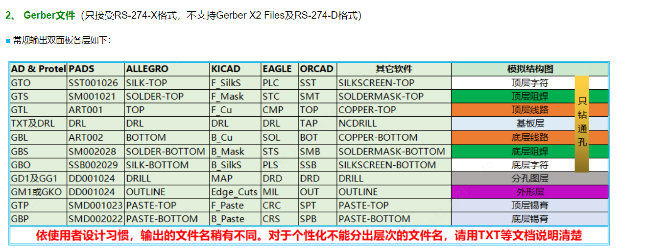
cadence官方教程
一个封装要包含这些部分: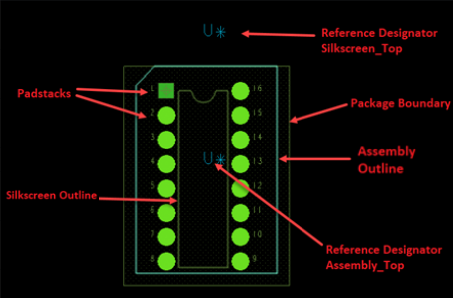
整理出表格为:
| 步骤 | class/subclass[5] | 备注 |
|---|---|---|
| Add and configure pins | Layout ─ Pins | For electrical pins, choose Connect. |
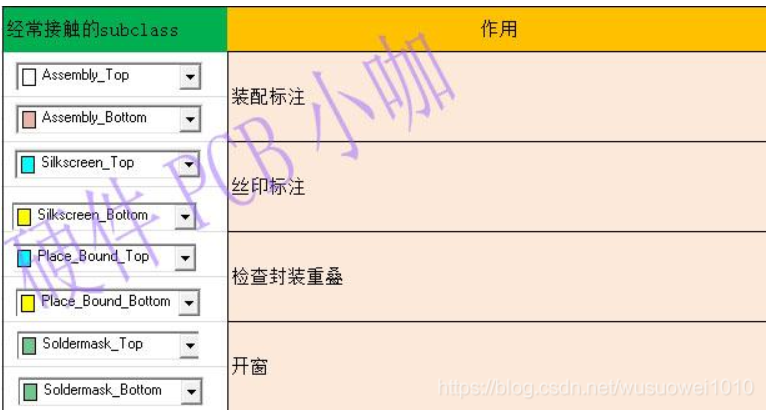
| Add component outlines | Silkscreen:Package Geometry class and Silkscreen_Top subclass | Silkscreen 丝印标注,白色的符号,不导电。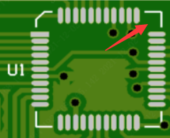 |
| Assembly:Package Geometry class and Assembly_top subclass | Assembly装配,专业装配安装图[1],普通用户一般看丝印。 |
|
| Define constraint areas | package boundary:Package Geometry class and Place_bound_top subclass | package boundary checks for package overlap and is used during placement 检测是否重叠,元件实际尺寸,防止元件和元件碰撞。 dfa_bound_Top [4] 如果不设置也会使用Place_bound_top。 |
| package height | Setup ─ Areas ─ Package Height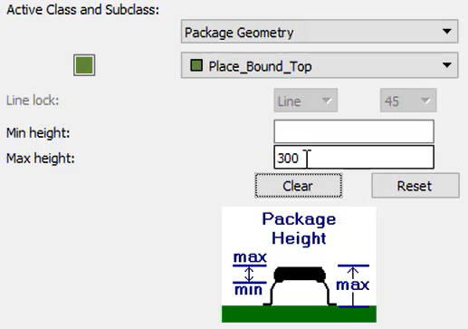 |
|
| Add labels Layout ─ Labels ─ RefDes 位号最少2个,一个丝印层,一个装配层。 |
Package Geometry class and Silkscreen_Top subclass | 位号,就是Q37这种元件标识。 写REF三个字母 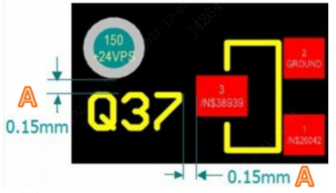 加logo、加第一个引脚的标识*。 |
| Package Geometry class and Assembly_top subclass | 装配图里的位号REF。 加第一个引脚的标识*。 |
|
| Save symbol files | N/A | .dra and .psm |
示例
我们以TI公司的LM311D为例,从ultralibrarian下载符合IPC-7351B standard的封装。话说能免费下载的封装不香吗?注意D8-L的L为最小封装,M为最大封装[2]。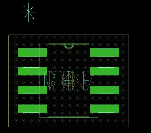
把上图拆开: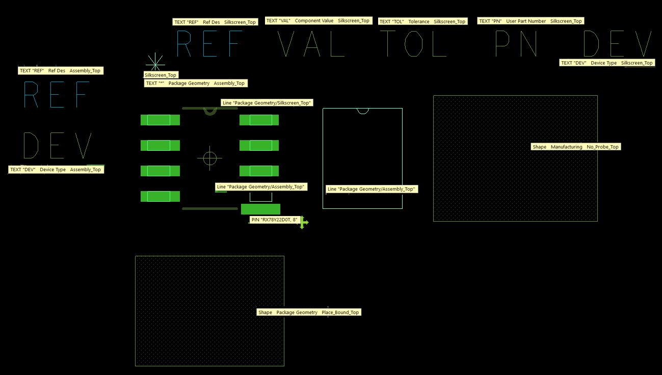
所以最重要的就是引脚、丝印信息、装配信息和位号。No_probe_top[3]是禁止探针探入区域。
参考资料
[1] The “assembly layer” is not something that gets included in the actual physical PCB, it’s just a drawing that becomes part of the documentation that accompanies it. The assembly drawing typically contains more detail than the silkscreen, and is used by the personnel who are assembling parts to the board (either directly or by programming a pick-and-place machine).The assembly layer is useful for setting up the pick and place machine in that you can make the reference designators very large and put them in the middle of the part so there is no confusion as to what part the refdes is for. You can also put large dots to indicate where pin 1 is. https://electronics.stackexchange.com/questions/204314/silkscreen-versus-assembly-layer
[2] LM311D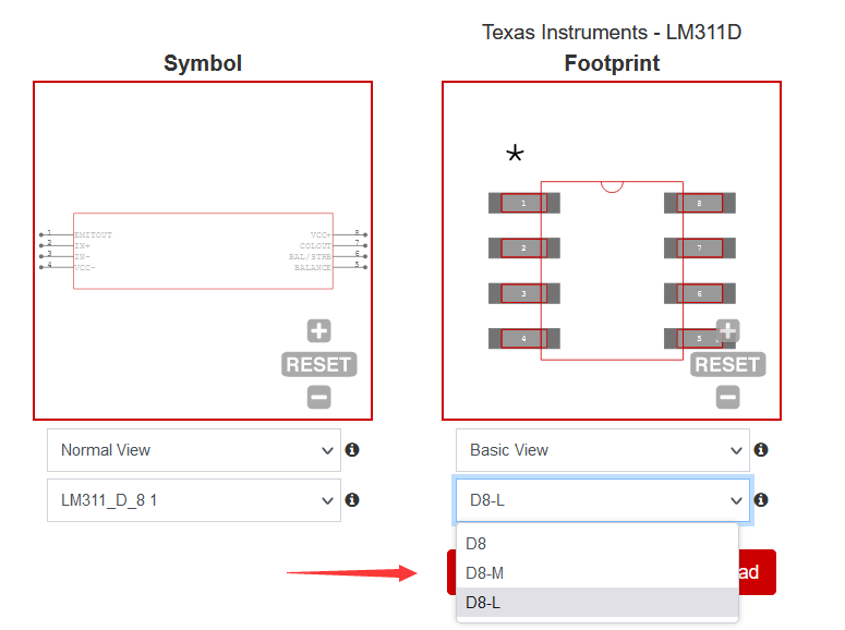
the L, M, N designators refer to the pad and footprint size. I believe these are from IPC-7351, but you need to pay for it.
- Least is 10% smaller than N; use for a really tight corner
- N is Nominal size
- Most is 10% larger than N; relaxed, good for hand assembly
All are compliant with the package size, so you can use any of them when laying out and the component will still fit.
[3]https://www.cnblogs.com/tongji-wu/p/3483867.html
[4] If this boundary does not exist than the DFA checks default to using the Place_Bound_Top boundary.
[5] https://blog.csdn.net/wusuowei1010/article/details/102620332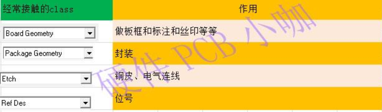

若有收获,就点个赞吧
0 人点赞
