Hardware 101
硬件 101
In this document
内容
This page provides an overview of the basic electronics concepts you should be familiar with to safely connect peripherals to devices and begin writing apps that bring them to life.
本页面综述了所需要熟悉的基本电子概念,以便安全地连接外设设备并开始写实际的应用程序。
You should have a basic understanding of the relationships between voltage, current, resistance, and power before moving on, so you might find DC Circuit Theory and Ohms Law and Power helpful if you need more detail on these topics first.
在进一步了解之前,需要对电压,电流,电阻和电源之间的关系有一个基本的理解,所以如果需要这些方面的更多细节,请参阅 直流电路理论 和 欧姆定律和电源 会有帮助。
Breadboards
面包板
Breadboards are a common tool for quickly prototyping circuits without needing to solder components together. This allows you to make wiring changes during development until the design is stable. Breadboards can also be useful in testing, by allowing you to connect instrumentation easily and probe various connections in the circuit.
面包板 是常用的用来快速做电路原型的工具,这样可以不用把原件焊接到一起。用面包板可以让您开发当中做线路改变直到电路设计稳定下来。
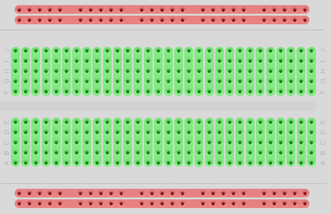
The holes of a breadboard are internally connected together in rows and columns to allow multiple components to share the same connection point. The outer rows are connected perpendicular to the rest of the board and form a single bus in each row across the top and bottom. These rows are typically used to connect power and ground, or other common signals needed across the entire circuit.
面包板的孔内部行列连到一起这样多个元件可以共用一个连接点。 最外边的行直连到整个板并在每一行形成一个单一的贯通总线。 这些行通常用来连接电源和地或者其他需要通过整个电路的信号。
Power supply
电源
Embedded devices contain active circuitry, which means they need an external power supply to function. Power is the input voltage delivered to the components on the board from an external source such as a wall adapter, battery, or USB port. The following signals are provided to the board by the power supply:
嵌入式设备包含有源电路, 这意味着它们需要电源来工作。电是从外部源如插座,电池或者 USB 口传过来到板上元件的输入电压。下面的信号由电源提供支持:
- VIN
- Voltage of the external source connected to the board. Many boards support a range of input voltages, and use an internal voltage regulator to provide stable power to the rest of the components.
- 连到板子的外部电压。很多板子支持一个范围内的输入电压, 并使用一个内部的 稳压源 给其他的元件提供稳定的电压。
- VCC or VDD
- VCC 或者 VDD
- Internal regulated voltage powering the components on the board. Common power supply voltages are +5V, +3.3V, and +1.8V.
- 内部稳压给板子上的元件供电。 通常的供电电压有 +5V, +3.3V, 和 +1.8V。
- Ground (GND)
- 地 (GND)
- Reference point for 0 volts on the board. All other voltages are measured with respect to ground. Voltages measured below ground are considered negative.
- 板子上的0伏参考点。所有其他电压参考地来测量。低于地的电压视为负电压。
To shut down a board, it is safe to disconnect the power supply. No special shut down procedures are necessary.
为了安全地关掉板子,断开电源就可以。不需要其他的特殊的步骤。
Analog and digital I/O
模拟和数字 I/O
Peripherals connect to your device using various input and output pins exposed on the board. Input pins allow your app to read and interpret the current electrical state. Output pins allow your app to control the electrical state of the pins. Peripherals and onboard I/O are either analog or digital in nature.
外设使用板子上裸露的不同的输入和输出 PIN 脚与板子相连。输入 PIN 脚允许应用读取和解释当前的状态。输出脚允许应用来控制 PIN 脚状态。外设和板上 I/O 本质上都是或者模拟或者数字的.
Analog
模拟
Analog devices produce voltage that’s proportional to the physical conditions they measure. A good example is a temperature sensor, which may produce an output between 0-5V corresponding to a temperature between 0-100°C.
模拟设备按照它们测量的物理条件来输出对应的电压。温度传感器就是一个很好的例子,它能按照相应的 0-100°C 产生一个在 0-5V 之间的输出电压。
Analog inputs translate a discrete voltage level into a proportional integer value using an analog-to-digital converter (ADC). The range of integers used to express the voltage level is based on the resolution of the ADC, expressed in bits. A 10-bit ADC, for example, can express the input voltage as a value between 0-1023 (for example, 210 discrete steps).
模拟输入使用 模数转换器 (ADC) 把离散的电压值转换成一个成比例的整数值。用来表示电压的整数范围基于按位表示的 ADC 的分辨率。例如,一个10位 ADC 可以表示在 0-1023 之间的值(如, 210 离散值).
Digital
数字
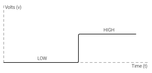
Digital logic represents a voltage signal as a binary value:
数字逻辑用二进制值来代表一个电压信号
High: When the voltage is at or near VCC. Typically represented as a logical “1”.
High: 当电压在或接近 VCC。 通常代表逻辑 “1”。
Low: When the voltage is at or near ground. Typically represented as a logical “0”.
Low: 当电压在或接近地。 通常代表逻辑 “0”。
It’s rare for a digital signal to be exactly 0V or VCC. Most digital logic devices interpret a range of voltages near the extremes as a valid logic level. The following table indicates common input voltage ranges for each logic state.
对一个数字信号来讲正好是 0V 或者 VCC的情况很少见到。大多数逻辑设备会把一定范围的接近这两个端值的电压作为有效的逻辑值。下面的表格表明每个逻辑值的通常的输入电压范围。
|
Supply Voltage (VCC) 供电电压 (VCC) |
Logic Low 逻辑低电压 (0) |
Logic High 逻辑高电压 (1) |
|---|---|---|
| 5V TTL | < 0.8V | > 2.0V |
| 3.3V CMOS | < 0.8V | > 2.0V |
| 1.8V CMOS | < 0.6V | > 1.2V |
Peripherals typically use digital I/O in a few common ways:
外设通常通过以下几种方式使用数字 I/O:
Stable state: Single on/off state mapped to a stable high or low value.
稳定状态: 单一的开/关状态 变到一个稳定的高或低压。
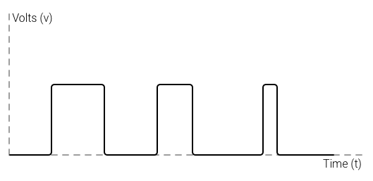
Pulse train: Series of digital signal pulses with variable frequency and width transmitted continuously over time.
脉冲序列: 一连串带可变频率和带宽的持续数字脉冲。
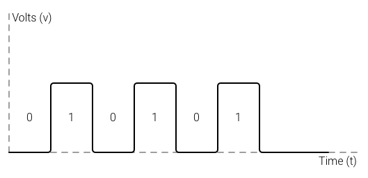
Serial communication: Series of digital 1s and 0s representing individual bits of a binary number.
串行通信: 一系列的 0 和 1 代表分别代表一个二进制数的某一位。
For more information on analog and digital I/O, see Sensors and Transducers and Binary Numbers.
想要了解关于模拟和数字 I/O 的更多信息, 可以参考 各种传感器和转换器 和 二进制数.
Pull-ups and pull-downs
上拉 和 下拉
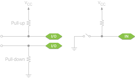
In many digital interface circuits, resistors are connected between the I/O signal pins and VCC or ground. These are known as pull-up and pull-down resistors, respectively. They guarantee that each signal has a stable default state that the rest of the system can rely on, without significantly affecting the input or output signal directly.
在许多数字接口电路中,电阻连在 I/O 信号脚 和 VCC 或者地之间。这就是所谓的上拉或下拉电阻。它们可以保证每个信号可以有个稳定的缺省状态,系统里其他部分可以依赖这个稳定状态,这样不会直接对输入或输出信号有明显的影响。
A digital input that is not actively connected to any signal is a floating input. Floating inputs are susceptible to electromagnetic interference, which affects the value reported to your app and causes unpredictable readings. Pull-up or pull-down resistors ensure that the line is driven to a stable value, even when nothing else is connected.
没有连到任何信号的数字输入是漂浮输入。漂浮输入容易遭受 电磁干扰, 电磁干扰会影响给应用的值使得应用读取的值不可预测。即使什么也不连,上拉和下拉电阻也可以确保电路被拉到一个稳定的值。
As an example, think of a button or switch. A switch is a pair of contacts that connects an input pin to a high or low voltage when closed, but leaves the input floating when open. In addition, many digital transducers use open collector (or open drain) outputs to report a state change. These outputs act like a simple switch and require and external source to drive the input when the switch is open.
作为一个例子,考虑一个按键或开关。开关是一对继电器,当关的时候连接一个输入 PIN 脚到一个高电压或低电压上,当开的时候输入处于漂浮态。另外,许多数字转换器使用 开集 (或开漏) 输出来报告状态改变。这些输入就如同一个简单开关,当开关打开时需要外部资源去驱动输入。
Resistor strength
电阻强度
The resistor values you choose affect the system in different ways. Low value resistors are considered “strong” because more current flows. Strong pull-ups (or pull-downs) draw more power overall, but they can reset the signal to an idle level more quickly than a “weak” resistor with a higher value.
选择的电阻值会以不同的方式影响系统。因为有更大的电流,低阻值电阻被看作“强”。总的来说强上拉(或下拉)吸引更多电,但它们比一个“弱”高阻值的电阻能更快地复位信号到闲置状态。
Note: Pull-up and pull-down resistor values are typically between 1kΩ and 10kΩ.
注意: 上拉和下拉电阻阻值一般在 1kΩ 和 10kΩ 之间
As an example, the I2C serial bus uses pull-up resistors to keep the clock and data lines stable when the bus is idle. Each device added to the bus loads down these lines, making it harder for the pull-up to keep the line at the appropriate level. As the number of devices on the bus increases, the strength of the pull-ups must also increase to handle the added load.
作为一个例子,I2C 串行总线在总线空闲时使用上拉电阻来保持时钟和数据信号稳定。每一个加到总线的设备会拉低这些信号,并使得上拉难以保持信号在合适的电平上。随着在总线上面的设备增加,上拉的力量必须加强以应对增加的负载。
See Pull-up Resistors for more details on applications and calculating the proper values.
参看 上拉电阻 可以了解到更多应用的细节并计算合适的值。
Signal debounce
信号去抖
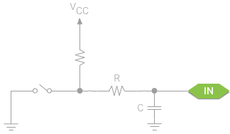
Many electrical input devices, such as switches and relays, have a mechanical component. As the mechanical motion of the device settles, the electrical signal can temporarily oscillate — or “bounce” — between multiple values. In many cases, this will be seen by your app as multiple input events in a very short time.
许多电子输入设备,如开关和继电器,有机械元件。随着该设备机械移动停下来,电信号会在多个值之间临时震荡或者说是”跳跃”。在大多数情况下,您的应用会认为系统在很短时间里触发了多个输入事件。
To correct this problem, you must debounce the signal using hardware or software. Software debounce involves setting a time delay between the initial input event and when the input is expected to stabilize (usually not more than a few hundred milliseconds).
为了修正这个问题,必须用硬件或软件来“去抖”。软件去抖涉及在初始的输入事件和输入稳定之间设定一个延迟时间(通常不超过几百微秒)。
To debounce your input with hardware, add a simple RC circuit (so-named because it contains a resistor and capacitor) between the input pin and the device. When the input device changes state, the capacitor will charge and discharge at a rate proportional to the size of the input resistor, effectively slowing down the transitions seen by the input pin.
为了用硬件去抖,在输入 PIN 脚和设备之间增加一个简单的 RC 电路(这样命名是因为它包含一个电阻和电容)。当输入设备改变状态,电容会以正比于输入阻抗的速率充电和放电,可以有效的减缓输入 PIN 脚的状态改变。
See Input Interfacing Circuits for more information on calculating debounce and other techniques for connecting input signals to your device.
参看 输入接口电路 相关信息,了解更多关于计算去抖和其他输入信号连到设备上的技术。
Protecting I/O pins
I/O 引脚保护
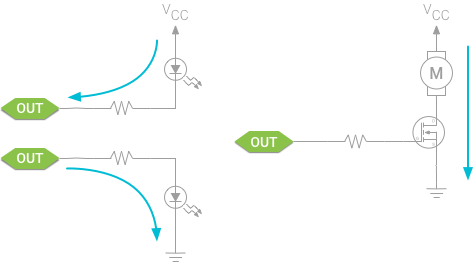
Each output pin has a limited capability to source (when high) or sink (when low) current from the circuitry connected to it. Peripherals that draw more current than the pin can handle — even temporarily — can damage the output. To protect the pin, insert a current-limiting resistor in series with the load.
每一个输出 PIN 脚有一个有限的能力从相连电路去拉电流(为高)或灌电流(为低)。外设能汲取的电流通常要比 PIN 脚能承受的电流要大 — 即使是短暂的大电流 — 也会破坏输出。为了保护 PIN 脚,所以插入一个限流带负载的串阻。
Note: Series resistor values are typically between 100Ω and 300Ω.
注意: 串阻值通常在 100Ω 和 300Ω 之间。
To control higher power transducers, such as motors, buffer the load from the output pin using a transistor or similar electronically controlled switch and power the transducer directly from the power supply.
为了控制高能变换器,例如马达,用一个晶体管做负载缓冲或简单的电子控制开关并从直接对变换器供电。
Note: The source/sink capacity of I/O pins will vary by device. Check your hardware documentation to better understand what your board can support.
注意: I/O PIN脚的拉/灌能力因设备而不同。 看您的硬件文档来更好的理解什么是您的板子能支持的。
All I/O pins are designed to safely operate with in the voltage range between 0V and VCC. Connecting any pin to a voltage higher than the power supply for that component will likely damage it. Always verify that the voltage levels generated by your sensors and transducers match their connected I/O pins. To connect devices of variable supplies together, use a logic level converter circuit.
所有的 I/O PIN脚设计成能在电压范围在 0V 和 VCC之间安全工作。连接任何 PIN 到一个高于元件供电电压时很可能会损害到该 PIN 脚。一定要验证您的传感器和转换器产生的电压能匹配跟它们连的 I/O PIN脚。为了连不同供电的设备到一起,用电平转换器 电路。
See Output Interfacing Circuits for more examples of circuits you can use to safely interface with digital and analog I/O.
参看 输出接口电路 可以找到更多能用来安全使用的数字和模拟 I/O 接口电路。

若有收获,就点个赞吧
0 人点赞
